

Nano-wire field effect transistor
A technology of field effect transistors and transistors, applied in semiconductor devices, electrical components, circuits, etc., to achieve the effects of increasing current switching ratio, improving performance, and reducing static power consumption
- Summary
- Abstract
- Description
- Claims
- Application Information
AI Technical Summary
Problems solved by technology
Method used
Image

Examples
Embodiment 1
[0019] Embodiment 1. Silicon nanowire field effect transistor with core-shell structure and its performance detection
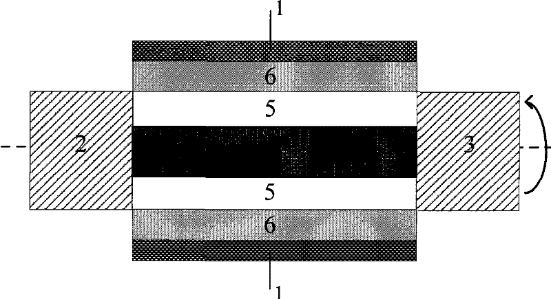
[0020] The structure of the nanowire field effect transistor is as follows figure 1 As shown, where the work function of the gate electrode 1 material is set to 4.61 electron volts, the source region 2 and the drain region 3 are doped with phosphorus at a concentration of 1×10 20 cm -3 silicon material, the core part 4 is silicon oxide, and the shell part 5 is boron doping concentration 1×10 11 cm -3 silicon material, and the gate dielectric layer 6 is silicon oxide with a thickness of 2nm. The shell radius of the core-shell structure is 10 nm, the length of the core-shell structure is 0.1 micron, and the core radius is adjustable.
[0021] The above-mentioned transistors can be prepared according to existing methods, and the preparation process is briefly described as follows:
[0022] 1) Etch the silicon pillars on the silicon wafer with a circular sil...
Embodiment 2
[0031] Embodiment 2, germanium nanowire field effect transistor with core-shell structure and its performance detection
[0032] The structure of the nanowire field effect transistor is still as figure 1 As shown, wherein, the work function of the gate electrode 1 material is set to 4.33 electron volts, the source region 2 and the drain region 3 are doped with arsenic concentration of 1×10 20 cm -3 germanium, the core part 4 is silicon oxide, and the shell part 5 is boron doping concentration 2×10 12 cm -3 germanium material, and the gate dielectric layer 6 is silicon oxide with a thickness of 1.5nm. The shell radius of the core-shell structure is set at 10 nm, the length of the core-shell structure is 100 nm, and the core radius is adjustable.
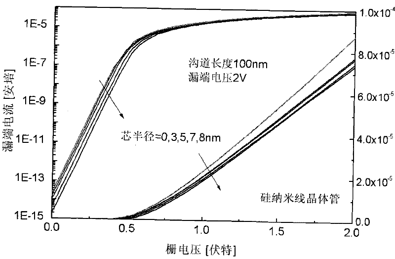
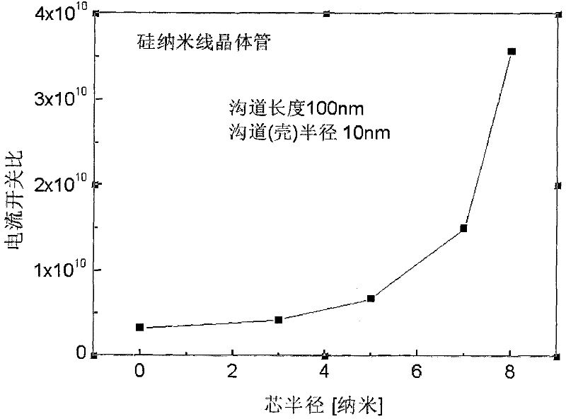
[0033] The current output characteristics, switching ratio, threshold voltage and leakage-induced barrier lowering effect of the transistor device were tested respectively, and the results obtained are as follows: Figure 6-Figur...
PUM
 Abstract
Description
Claims
Application Information