Substrate placement unit
A substrate and tray technology, which is applied in the manufacture of electrical components, electrical solid devices, semiconductor/solid devices, etc., can solve the problems of rising tray manufacturing costs, widening intervals, increasing tray deformation, etc., to minimize temperature deviation, Effect of preventing temperature deviation and improving tray life
- Summary
- Abstract
- Description
- Claims
- Application Information
AI Technical Summary
Problems solved by technology
Method used
Image
Examples
Embodiment Construction
[0053] Preferred embodiments of the present invention will be described in detail below with reference to the accompanying drawings, but the present invention is not limited or limited by the embodiments. For reference, in this description, the same symbols refer to substantially the same elements, under this rule, the content recorded in other drawings can be cited for description, and it can be omitted. Obvious or repetitive content.
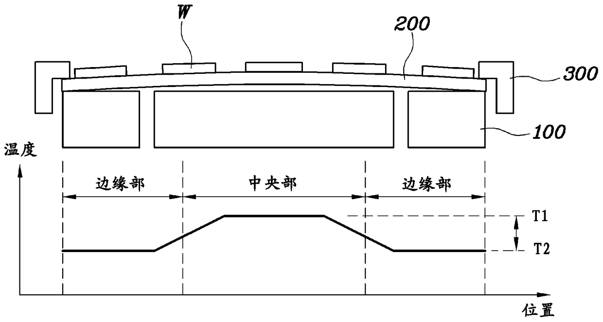
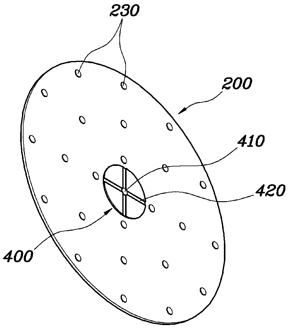
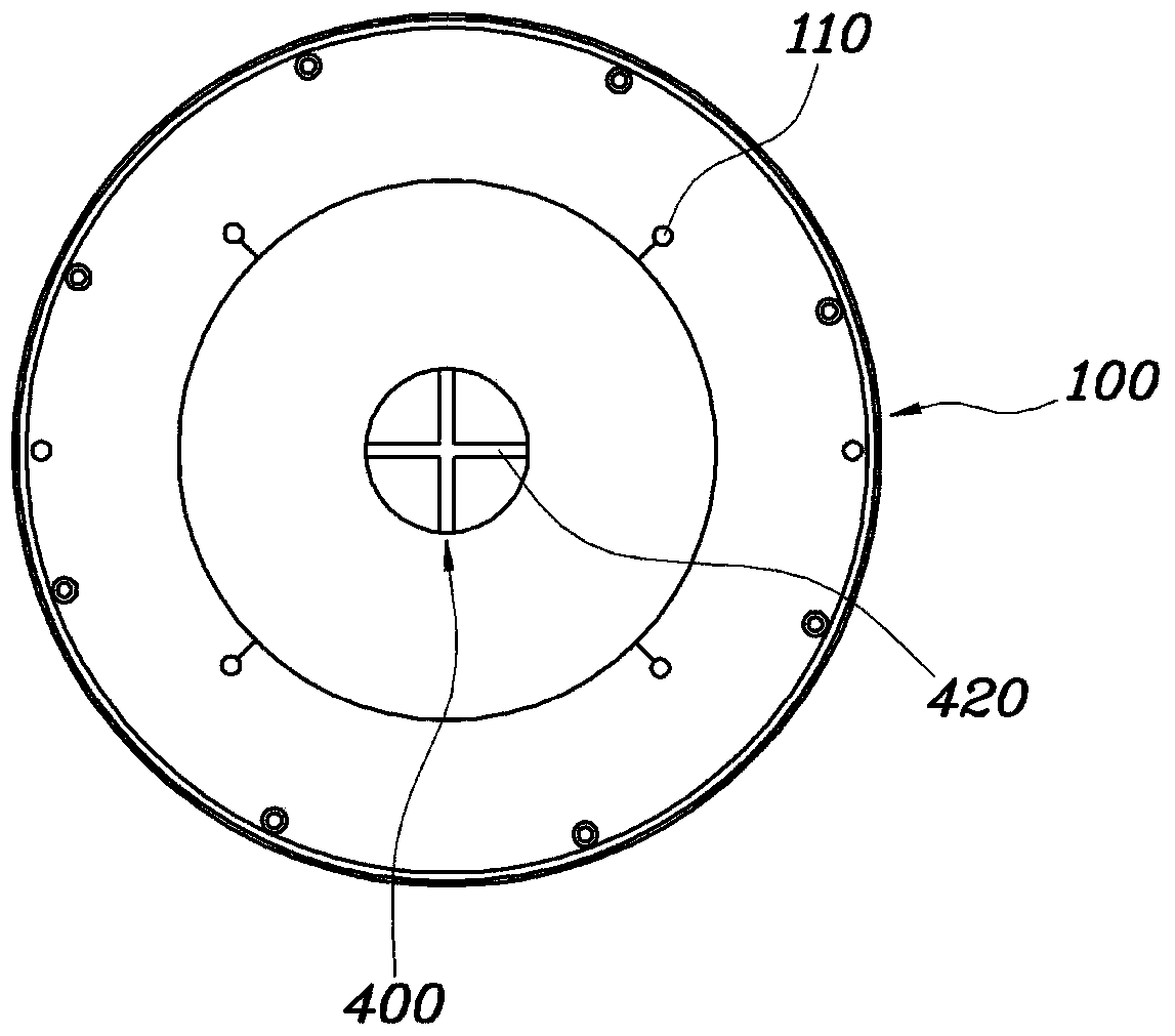
[0054] The substrate placement unit in one embodiment of the present invention includes: a chuck 100, which is arranged inside the cavity of the substrate processing device; a tray 200, which is placed on the upper part of the chuck 100, and a plurality of substrates W are placed on its plane; and clamps 300, which makes the tray 200 and the chuck 100 combined and fixed.
[0055] It is characterized in that when clamps 300 are used to press and fix the edges of the chuck 100 and the tray 200, the center of the tray 200 is deformed to be conve...
PUM
 Abstract
Description
Claims
Application Information


