A silicon-based plasmonic ultra-broadband terahertz wave absorber
A plasma, ultra-broadband technology, applied in antennas, electrical components, etc., can solve the problems of insufficient bandwidth and low absorption efficiency of terahertz wave absorbers, achieve broad application prospects and application value, reduce manufacturing costs, and simplify processes. The effect of the process
- Summary
- Abstract
- Description
- Claims
- Application Information
AI Technical Summary
Problems solved by technology
Method used
Image
Examples
Embodiment Construction
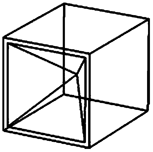
[0026] Such as figure 1 As shown, a silicon-based plasma ultra-broadband terahertz wave absorber proposed by the present invention includes basic units arranged in a moment periodic arrangement, and the basic units are seamlessly connected.
[0027] Such as figure 2 As shown, the basic unit is a rectangular parallelepiped with a square front and a concave quadrangular pyramid on the front. The concave quadrangular pyramid is mainly used to generate the plasmon resonance effect, so that the incident terahertz wave is confined in the structure, and then dissipated by the ohmic loss of the semiconductor material.
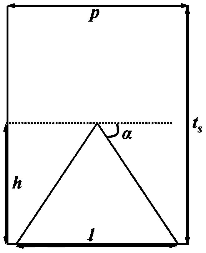
[0028] Such as image 3 As shown, the periodic length p of the basic unit is 50-300 μm, the thickness t s 50-500μm, the notch length l of the quadrangular pyramid is 48-290μm, the notch depth h is 25-250μm, and the inclination angle α≥20°, where l≤p, hs , preferably, the notch depth h of the quadrangular pyramid is the thickness t of the basic unit s The size para...
PUM
 Abstract
Description
Claims
Application Information


