Supercharge Your Innovation With Domain-Expert AI Agents!

Manufacture method adopting inner layer pattern transfer exposure

A production method and technology of inner layer graphics, applied in the direction of pattern and photolithography, multilayer circuit manufacturing, pattern formation through transfer, etc., can solve the problems of scrapping the whole board, misalignment between the graphics layers on both sides, etc., and achieve convenient and simple operation Effect

Inactive Publication Date: 2016-05-25
谢兴龙
View PDF5 Cites 5 Cited by
  • Summary
  • Abstract
  • Description
  • Claims
  • Application Information

AI Technical Summary

Problems solved by technology

[0002] In the PCB industry, during the transfer of the inner layer graphics of the multilayer board, the circuit graphics are exposed on both sides of the substrate with film negatives, and then the circuit is etched by negative etching, but since there is no reference point on both sides of the substrate Therefore, if the operation is not done properly, it is very easy to cause misalignment between the graphics layers on both sides, which will lead to the scrapping of the entire board

Method used


Image

  • Manufacture method adopting inner layer pattern transfer exposure
  • Manufacture method adopting inner layer pattern transfer exposure
  • Manufacture method adopting inner layer pattern transfer exposure

Examples


Embodiment Construction

[0024] The technical features of the present invention will be described in further detail below in conjunction with the accompanying drawings so that those skilled in the art can understand.

[0025] A method for making an inner layer graphic transfer exposure, comprising the following steps:

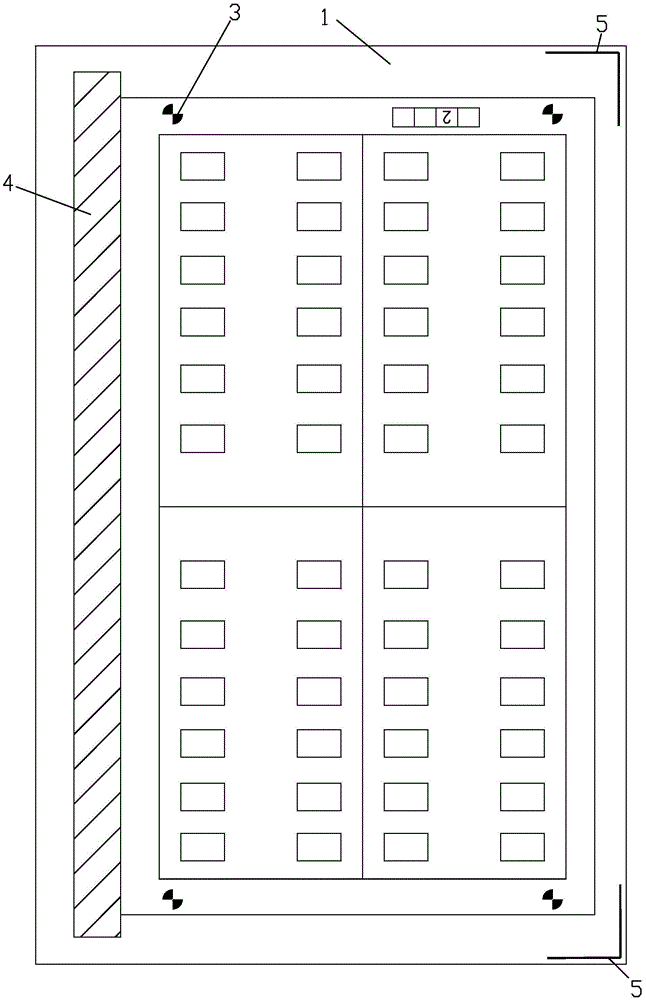
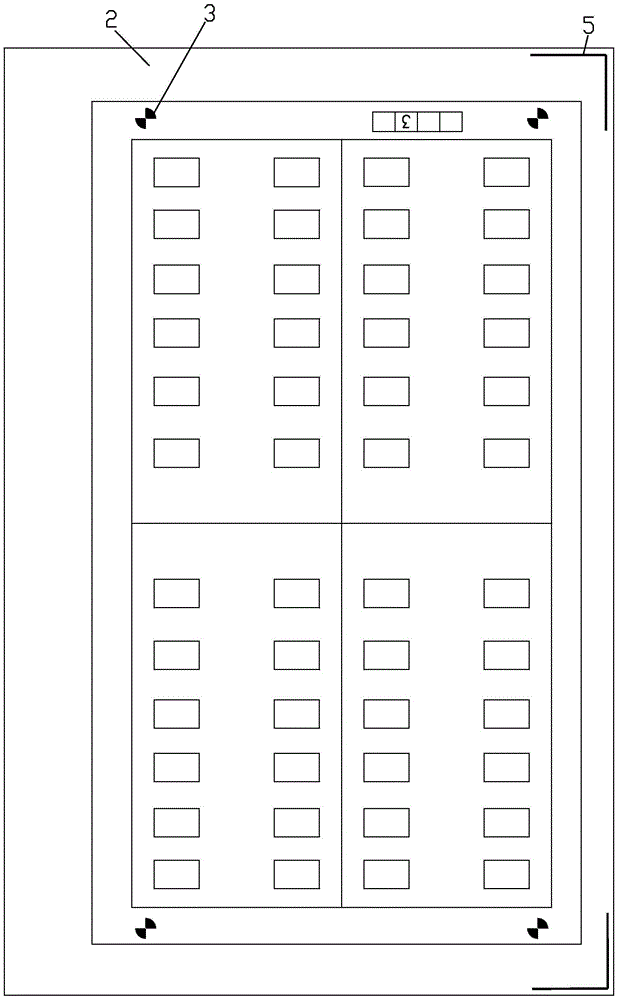
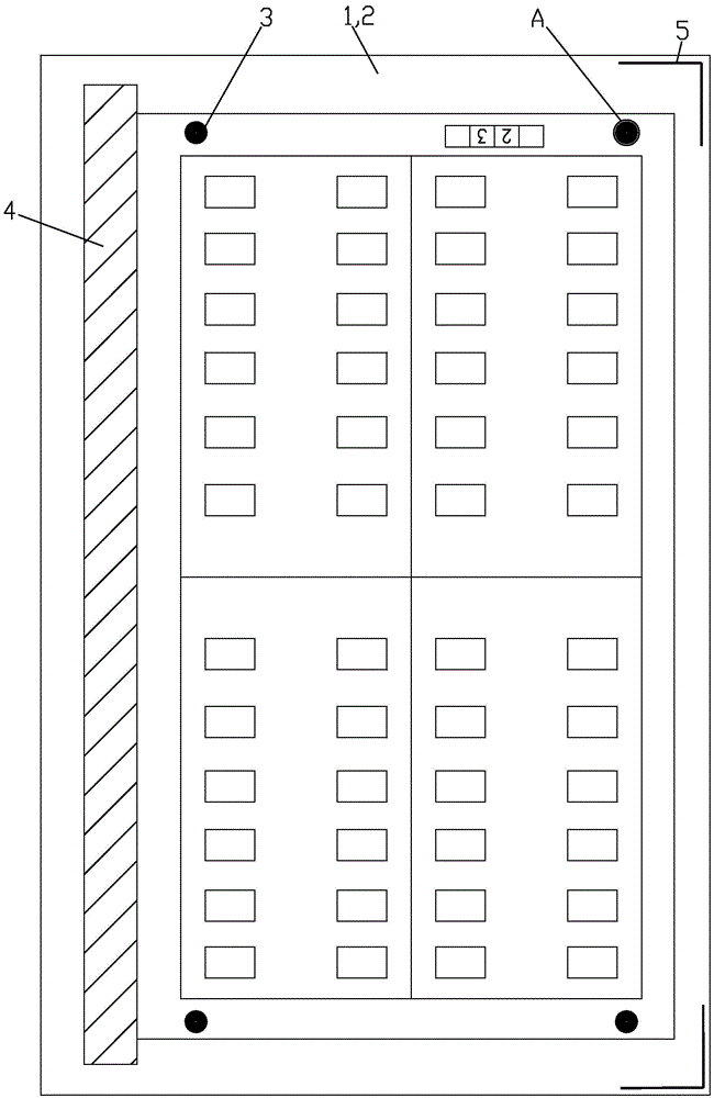
[0026] A. Film production, use CAM to design two films: the lower film 1 and the upper film 2, the circuit board to be exposed is sandwiched between the two films for exposure, and at least three corners of the effective area of ​​the two-sided exposure film are added respectively. Butterfly-shaped PAD3, said butterfly-shaped PAD3 is an image developed on a film;

[0027] B. Carry out film "sandwich" production: stick the bottom of the auxiliary side strip 4 to the periphery of the lower film 1 through double-sided adhesive tape, and stick double-sided adhesive tape on the top of the auxiliary side strip 4;

[0028] C. Align the upper film 2 with the lower film 1 until the correspondi...


PUM


Abstract

The invention discloses a manufacture method adopting inner layer pattern transfer exposure. According to the technical schemes of the invention, the method includes the following steps that: a butterfly-shaped pad is arranged at least three corners of the periphery of each of an upper film and a lower film; the bottom of an auxiliary edge bar is bonded to the periphery of the lower film through a double-sided adhesive tape, and a double-sided adhesive tape is bonded to the top of the auxiliary edge bar; the upper film and the lower film are aligned with each other until corresponding butterfly-shaped pads on the two films form a circular structure; and the upper film is bonded on the top of the auxiliary edge bar; and a circuit board to be exposed is arranged in a space between the two films so as to be exposed. The method is simple and convenient in operation. With the method adopted, the manufacture of a film sandwich can be quickly completed. When the method is used to perform exposure, board scrapping caused by inter-layer misalignment can be avoided, and quality can be improved significantly.

Description

【Technical field】 [0001] The invention relates to a method for making inner layer pattern transfer exposure. 【Background technique】 [0002] In the PCB industry, during the transfer of the inner layer graphics of the multilayer board, the circuit graphics are exposed on both sides of the substrate with film negatives, and then the circuit is etched by negative etching, but since there is no reference point on both sides of the substrate Therefore, if the operation is not done properly, it is very easy to cause misalignment between the graphics layers on both sides, which will lead to the scrapping of the entire board. [0003] The present invention is made based on this situation. 【Content of invention】 [0004] The object of the present invention is to overcome the deficiencies of the prior art, and provide a method for making inner layer pattern transfer exposure, so as to achieve the purpose of improving product yield and reducing scrap. [0005] The present invention...

Claims


Application Information

Patent Timeline
IPC IPC(8): H05K3/46
CPCH05K3/46H05K2203/0528
Inventor 谢兴龙欧伟祺
Owner 谢兴龙
Features
  • R&D
  • Intellectual Property
  • Life Sciences
  • Materials
  • Tech Scout
  • Unparalleled Data Quality
  • Higher Quality Content
  • 60% Fewer Hallucinations
Learn More