Supercharge Your Innovation With Domain-Expert AI Agents!

Formation method of TEM sample

A technology for transmission electron microscope samples and samples, which is applied in the field of semiconductor manufacturing, can solve the problems of destroying the complete wafer, the accuracy cannot meet the detection requirements, etc., and achieves the effect of accurate size

Active Publication Date: 2019-04-26
SEMICON MFG INT (SHANGHAI) CORP
View PDF8 Cites 0 Cited by
  • Summary
  • Abstract
  • Description
  • Claims
  • Application Information

AI Technical Summary

Problems solved by technology

[0005] However, the above-mentioned method of forming samples will completely destroy the complete wafer. Moreover, with the reduction of the size of semiconductor devices and the improvement of integration, the accuracy of the formed samples can no longer meet the detection requirements. Therefore, it is necessary to seek more accurate sample formation. Method to reduce damage to wafer integrity and improve dimensional accuracy of formed samples

Method used


Image

  • Formation method of TEM sample
  • Formation method of TEM sample
  • Formation method of TEM sample

Examples


Embodiment Construction

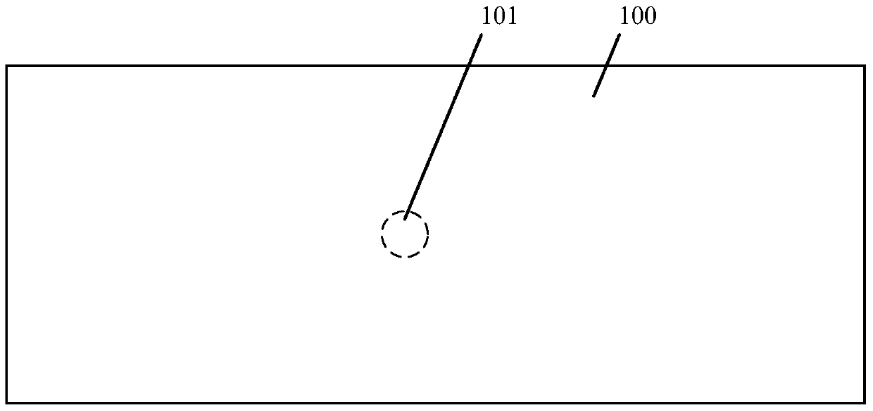
[0028] As mentioned in the background art, the existing method for forming samples will completely destroy the complete wafer, and the precision of the formed sample size is poor.

[0029] After research, it is found that in the existing sample preparation process, in order to obtain the primary sample, the wafer needs to be diced, and only part of the wafer including the target area in the wafer is reserved. Therefore, in order to obtain the primary sample, the complete If the wafer is completely destroyed, the wafer can no longer be used for other processes or inspections except for transmission electron microscope inspection, so that the utilization rate of the wafer is low, and the cost of the transmission electron microscope inspection is too high .

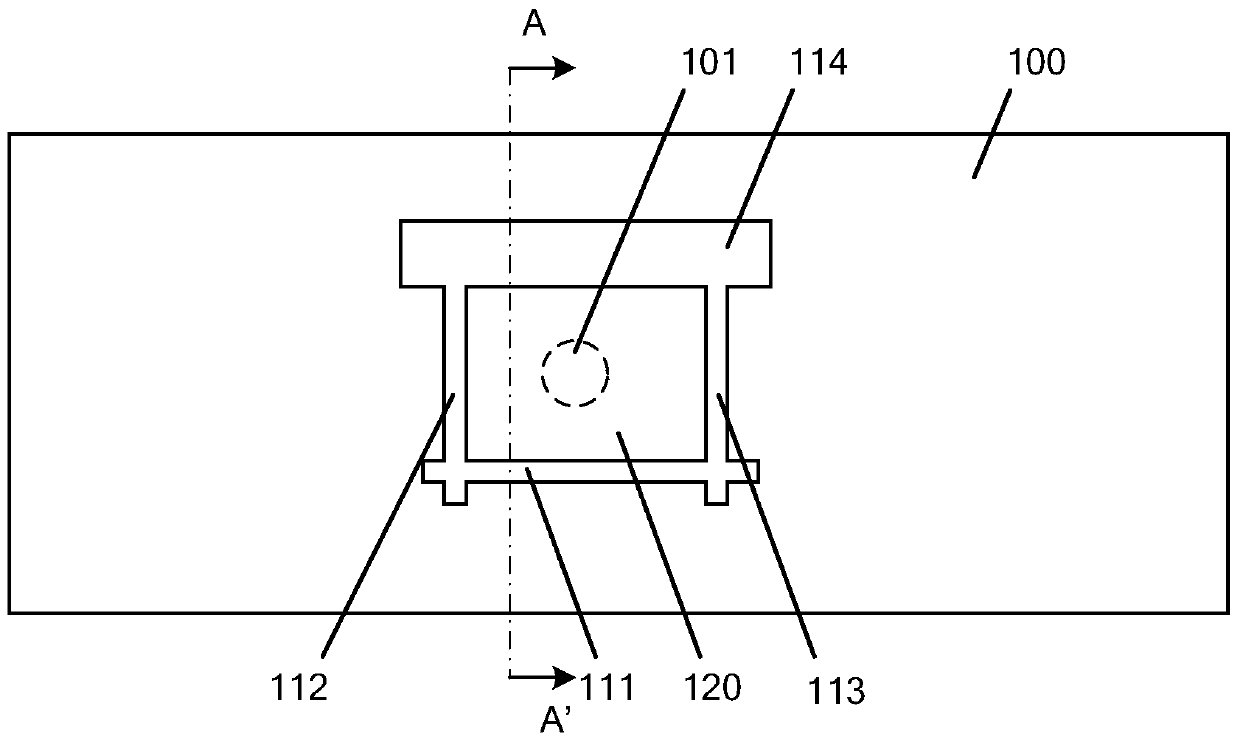
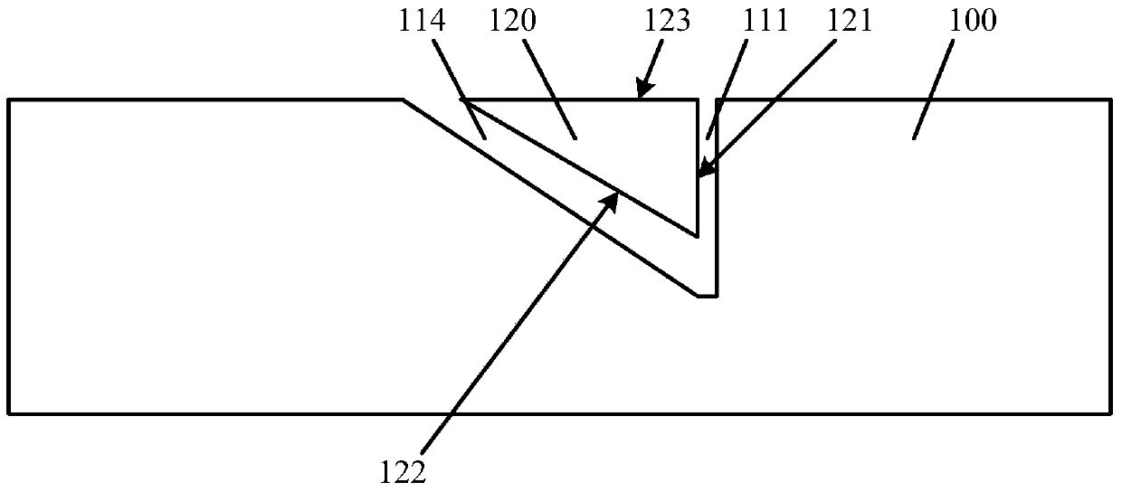
[0030] Moreover, in the existing sample preparation process, processes such as forming the first cutting mark, dicing the wafer, forming the grinding mark, grinding the primary sample, and finely grinding the surface of the ...


PUM

PropertyMeasurementUnit
lengthaaaaaaaaaa

Abstract

The invention discloses a transmission electron microscope sample forming method. According to the transmission electron microscope sample forming method, a substrate is provided, and a defect area is in the substrate; a first groove, a second groove, a third groove, and a fourth groove are formed in the substrate around the defect area; the part of the substrate surrounded by the first groove, the second groove, the third groove, and the fourth groove is a sample to be pretreated; an opening is formed in the sample to be pretreated; the top of the opening is on a second surface; the opening comprises a first side wall, and the first side wall is parallel to a surface to be detected; the first side wall is subjected to thinning until the distance from the first side wall to the surface to be detected is equal to a preset distance; after thinning of the first side wall, a cut penetrating the first side wall and the surface to be detected is formed; a sample to be detected is formed via surrounding of the sample to be pretreated by the cut; the sample to be detected comprises the defect area; and the sample to be detected is separated from the sample to be pretreated. The transmission electron microscope sample forming method is capable of ensuring wafer completeness, and accuracy of sample forming.

Description

technical field [0001] The invention relates to the technical field of semiconductor manufacturing, in particular to a method for forming a transmission electron microscope sample. Background technique [0002] In the semiconductor manufacturing industry, there are a variety of inspection equipment, among which the electron microscope is an important tool for inspecting the morphology, size and characteristics of the thin film during composition. Commonly used electron microscopes include transmission electron microscope (Transmission Electron Microscope, TEM for short) and scanning electron microscope (Scanning Electron Microscope, SEM for short). The working principle of the transmission electron microscope includes: putting the sample to be tested into the transmission electron microscope observation room, irradiating the sample with a high-voltage accelerated electron beam, enlarging the sample shape and projecting it on the screen, and completing the photography, and th...

Claims


Application Information

Patent Timeline
Patent Type & Authority Patents(China)
IPC IPC(8): G01N1/28
Inventor 赵燕丽段淑卿甄彦琳王莎
Owner SEMICON MFG INT (SHANGHAI) CORP
Features
  • R&D
  • Intellectual Property
  • Life Sciences
  • Materials
  • Tech Scout
  • Unparalleled Data Quality
  • Higher Quality Content
  • 60% Fewer Hallucinations
Learn More