Semiconductor Wafer Bump Structure

A bump structure, semiconductor technology, applied in the direction of semiconductor devices, semiconductor/solid-state device manufacturing, semiconductor/solid-state device components, etc. Problems such as delamination between the tops of wiring metal layers to reduce wafer warpage, avoid electrical performance failures, and avoid semiconductor device failures

Active Publication Date: 2018-03-27
NANTONG FUJITSU MICROELECTRONICS
View PDF6 Cites 0 Cited by
  • Summary
  • Abstract
  • Description
  • Claims
  • Application Information

AI Technical Summary

Problems solved by technology

However, when the thickness of the rewiring metal layer of the semiconductor wafer bump structure exceeds 10um, it is easy to form warpage during the packaging process, and the warpage degree is above 2mm, and can even reach 4mm, which cannot realize the large-scale manufacturing of semiconductor wafer level packaging. Production requirements; at the same time, it is easy to form a delamination between the bottom of the re-engineered passivation layer and the top of the re-wiring metal layer during the subsequent deterioration test, and this product is likely to cause subsequent electrical performance failure; in addition, for high-speed dedicated semiconductor devices Although this packaging structure meets the requirements of the flip-chip packaging structure structurally, it does not avoid the semiconductor device failure caused by the influence of α-rays in the metal solder on the circuit in the semiconductor chip to the greatest extent.

Method used


Image

  • Semiconductor Wafer Bump Structure
  • Semiconductor Wafer Bump Structure
  • Semiconductor Wafer Bump Structure

Examples


Embodiment Construction

[0014] The application will be further described in detail below in conjunction with the accompanying drawings and embodiments. It should be understood that the specific embodiments described here are only used to explain related inventions, rather than to limit the invention. It should also be noted that, for ease of description, only parts related to the invention are shown in the drawings.

[0015] It should be noted that, in the case of no conflict, the embodiments in the present application and the features in the embodiments can be combined with each other. The present application will be described in detail below with reference to the accompanying drawings and embodiments.

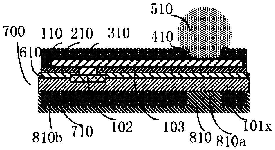
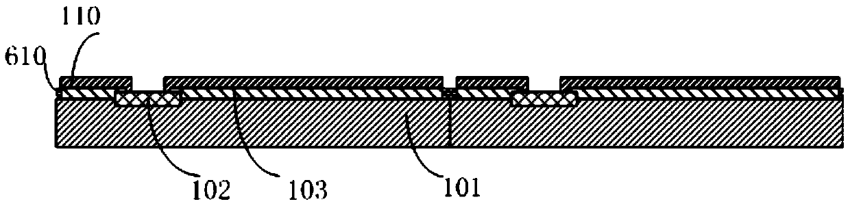
[0016] refer to figure 1 , the semiconductor wafer bump structure of the embodiment of the present invention includes:

[0017] Wafer 101X;

[0018] A recreated passivation layer formed on the upper surface of the wafer 101X;

[0019] A polymer material layer 710 formed on the lower surface of ...


PUM


Abstract

The present invention provides a semiconductor wafer bump structure, which comprises: a wafer; a recreated passivation layer formed on the upper surface of the wafer; a polymer material layer formed on the lower surface of the wafer; a layer formed on the polymer material layer Adhesive layer on each exposed side. Compared with the prior art, the method for forming the bump structure of the semiconductor wafer provided by the present invention can weaken the warping of the wafer, thereby facilitating the manufacture of processes such as testing before dicing, printing, and ball planting.

Description

technical field [0001] The invention relates to the technical field of semiconductors, in particular to a semiconductor wafer bump structure. Background technique [0002] In recent years, under the joint promotion of the cost reduction and the improvement of the front-end wafer manufacturing process of semiconductor devices, the single chip size of semiconductor devices with the same function has become smaller and smaller, and can be formed directly on the semiconductor wafer. Ball bumps mounted on printed circuit boards can be applied. Due to the limitations of the semiconductor wafer manufacturing process or the designer's consideration of multiple uses of the same integrated circuit, it is necessary to redefine the position of the input terminal for transmitting electrical signals to form a ball bump during semiconductor wafer level packaging, which requires metal rewiring structure. However, when the thickness of the rewiring metal layer of the semiconductor wafer bu...

Claims


Application Information

Patent Timeline
Patent Type & Authority Patents(China)
IPC IPC(8): H01L23/31H01L23/485H01L21/56H01L21/60
CPCH01L21/56H01L23/3171H01L24/11H01L24/13H01L2224/11H01L2224/13024H01L2224/05008H01L2224/05569H01L2224/13022H01L2224/94H01L2924/10253H01L2924/3511H01L2224/03
Inventor 施建根
Owner NANTONG FUJITSU MICROELECTRONICS
Why Eureka
Try Eureka