SEM transmission electron Kikuchi diffraction apparatus and analytical method

A technology of transmission electron and Kikuchi diffraction, which is applied in the field of materials, can solve the problems of inability to analyze nanoparticles, poor spatial resolution, and poor measurement accuracy of unit cell parameters, so as to expand the application space, solve large distances, and shorten working distances. Effect

Inactive Publication Date: 2016-06-08
SHANGHAI INST OF CERAMIC CHEM & TECH CHINESE ACAD OF SCI
View PDF5 Cites 20 Cited by
  • Summary
  • Abstract
  • Description
  • Claims
  • Application Information

AI Technical Summary

Problems solved by technology

[0006] (4) The measurement accuracy of unit cell parameters is poor, and it is necessary to rely on Energy Dispersive Spectrometry (EDS) or Wavelength Dispersive Spectroscopy (WDS) to perform more accurate phase identification
[0007] (5) Poor spatial resolution
However, there are few reports on the application of EBSD to non-conductive inorganic non-metallic materials.
The accelerating voltage of traditional EBSD analysis is 20kV, the range of action between the incident electron and the bulk sample is relatively large, the spatial resolution of EBSD is poor, about 150nm, and the orientation and crystallographic information at the nanometer scale cannot be analyzed; and EBSD must require the sample to

Method used


Image

  • SEM transmission electron Kikuchi diffraction apparatus and analytical method
  • SEM transmission electron Kikuchi diffraction apparatus and analytical method
  • SEM transmission electron Kikuchi diffraction apparatus and analytical method

Examples


Embodiment 1

[0062] Example 1: t-EBSD characterization of zirconia nanocoatings

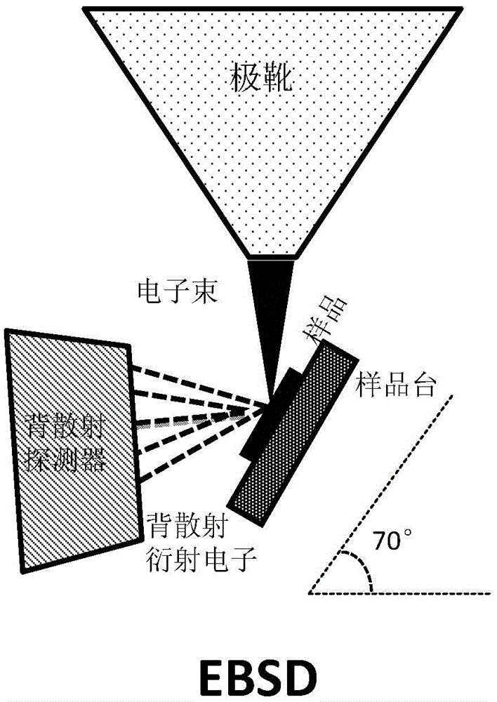
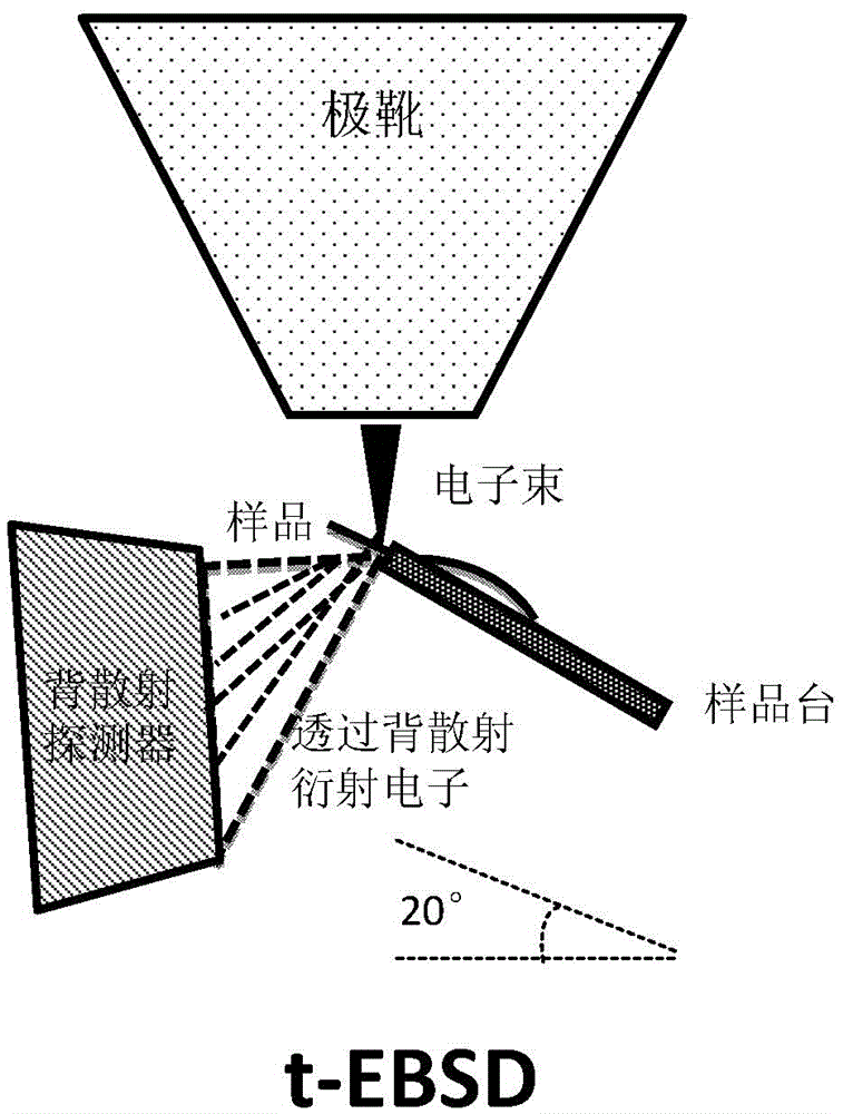
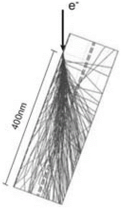
[0063] Thermal barrier zirconia coatings are widely used in hot-end components such as blades of aero-engines. Its low thermal conductivity reduces the thermal load on the substrate, protects the substrate and prolongs its service life. Understanding the grain phase composition and size distribution of thermal barrier zirconia coatings plays a crucial role in improving its service performance. The ion-thinned zirconia coating was characterized by t-EBSD, the backscattered electron diffraction voltage was 30kV, the current was 6.4nA, and the working distance was 1mm. Figure 8 The characterization results shown. The inconsistency of the thickness of the sample causes the band contrast of each region of the sample to be different, and the smallest diameter is only 30nm ((ZrO 2 ) 0.88 (Y 2 o 3 ) 0.12 ) grains. and according to Figure 9 , the average MAD of t-EBSD is 0.38°, indicating that the Kikuchi di...

Embodiment 2

[0064] Embodiment 2: t-EBSD characterization of titanium oxide nanopowder

[0065] TiO 2It is a material widely used in the field of photocatalysis, and its common crystal form is anatase and rutile with better photocatalytic performance. Grain size is the effect of TiO 2 An important factor of photocatalytic activity, the smaller the crystal grain, the more fully exposed the crystal active center, which is conducive to the improvement of catalytic activity; at the same time, the photogenerated carriers of small grains are easier to diffuse from the inside of the grains than large grains. Migrating to the surface is beneficial to promote the generation of the reaction and improve the photocatalytic efficiency. Therefore, for nanoscale TiO 2 The characterization of the grain size and crystal form of the particles is of great significance for the study of its photocatalytic performance.

[0066] Figure 11 is TiO 2 The secondary electron image of the nanopowder, a small gr...


PUM


Abstract

The invention provides a SEM transmission electron Kikuchi diffraction apparatus and an analytical method. The apparatus comprises the following components: an electron beam irradiation unit for irradiating electron beams on a sample; an electron backscatter diffraction detector and a sample stage which are located below the electron beam irradiation unit; wherein the sample stage is configured, so that an inclination angle is formed between the sample which is carried on the sample stage and a horizontal plane; and the detector is provided with a phosphor screen which is configured for acquisition and reception of transmission electron signals which are emitted by the sample. Clear transmission electron Kikuchi diffraction patterns are obtained, in order to realize phase identification and phase proportion calculation of crystal grains of nanometer scale, analysis of nanometer scale texture and misorientation, analysis of crystal grain size and shape, analysis of crystal boundary as well as properties of sub-grain and twin crystal, etc.

Description

technical field [0001] The invention relates to microstructure analysis equipment in the field of materials, in particular to a transmission electron Kikuchi diffraction device and analysis method in a scanning electron microscope. Background technique [0002] Field emission scanning electron microscope (FESEM) is a microstructure analysis equipment widely used in the field of materials at home and abroad. It can not only characterize the microstructure of inorganic non-metallic materials in a state close to the original state (non-coated conductive film state), but also qualitative , Quantitatively measure the chemical composition and structural information in the microscopic area, and provide scientific basis for the research and development of advanced materials, performance improvement, failure analysis, etc. The existing FESEM analysis method for material crystallography is backscattered electron diffraction (Electron Backscatter Diffraction, EBSD). Through the Kikuchi...

Claims


Application Information

Patent Timeline
IPC IPC(8): G01N23/04G01N15/00G01N15/02
CPCG01N23/04G01N15/00G01N15/02G01N2015/0038
Inventor 华佳捷林初城王墉哲刘紫微姜彩芬曾毅
Owner SHANGHAI INST OF CERAMIC CHEM & TECH CHINESE ACAD OF SCI
Why Eureka
Try Eureka