[0005]Exemplary embodiments and / or exemplary methods of the present invention are directed to providing a miniaturized terahertz radiation source, which is based on the Smith-Purcell effect, on a
semiconductor chip, using available additive
nanolithography, which may function as a miniaturized,
free electron laser, be substantially more powerful than existing such radiation sources, and facilitate a substantially broader field of application, in particular for analytical applications.
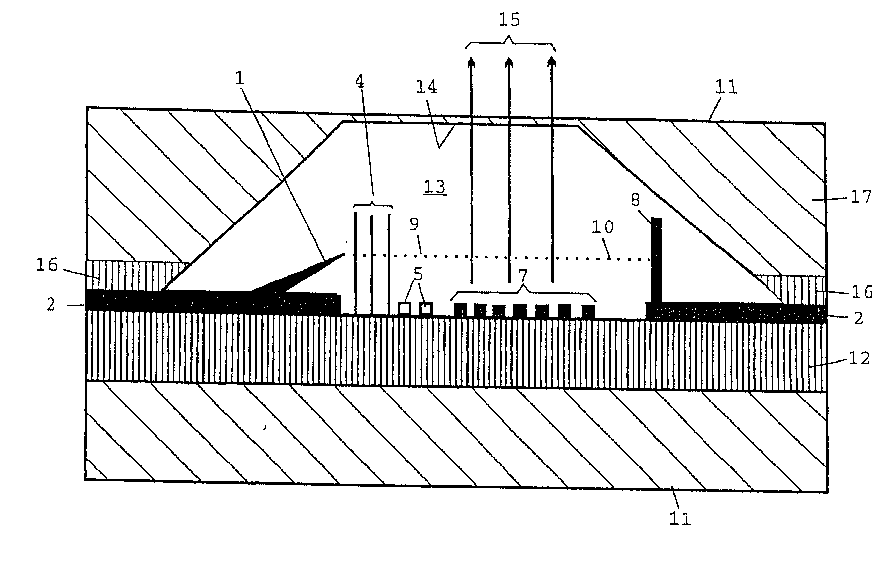
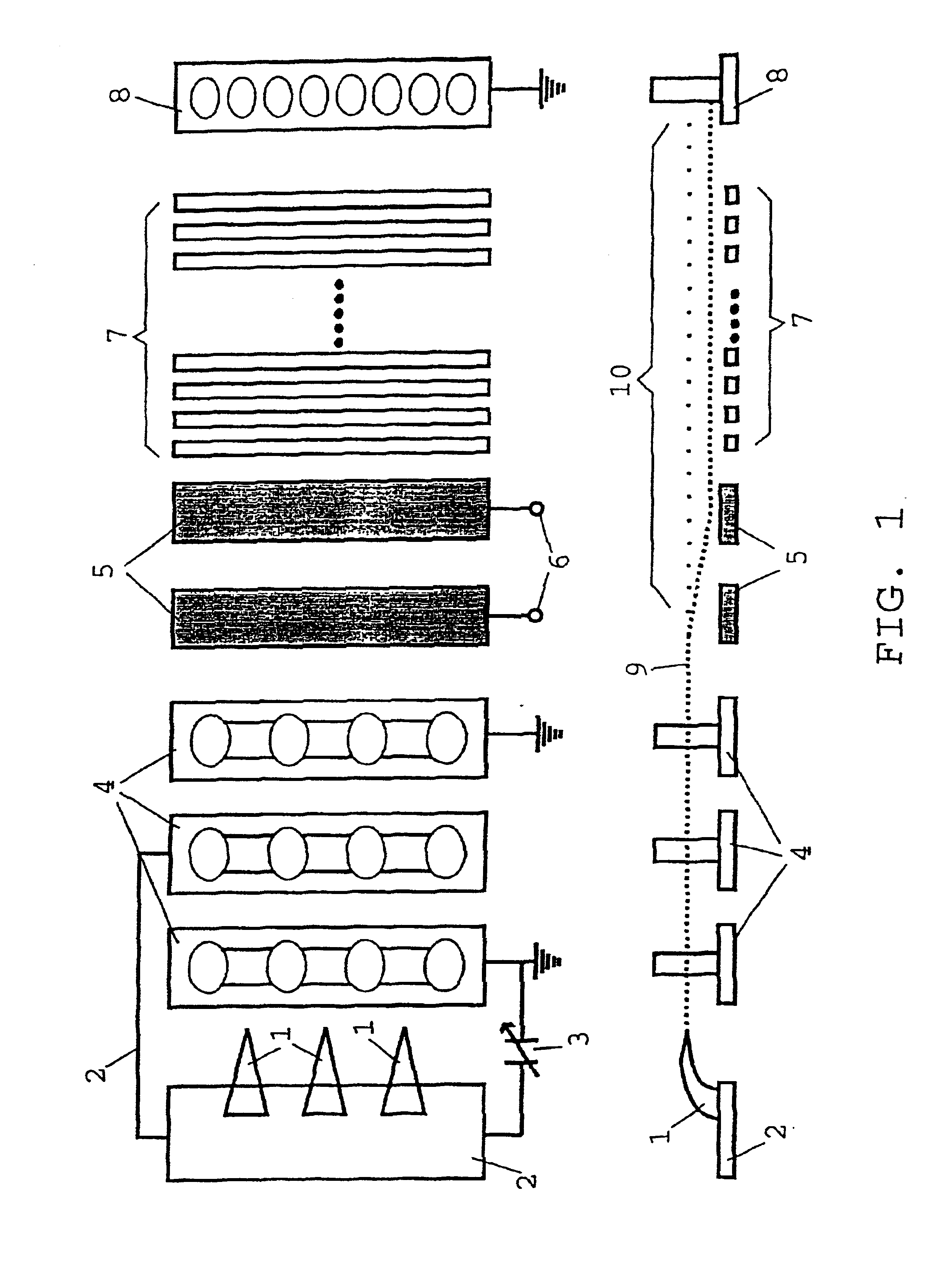
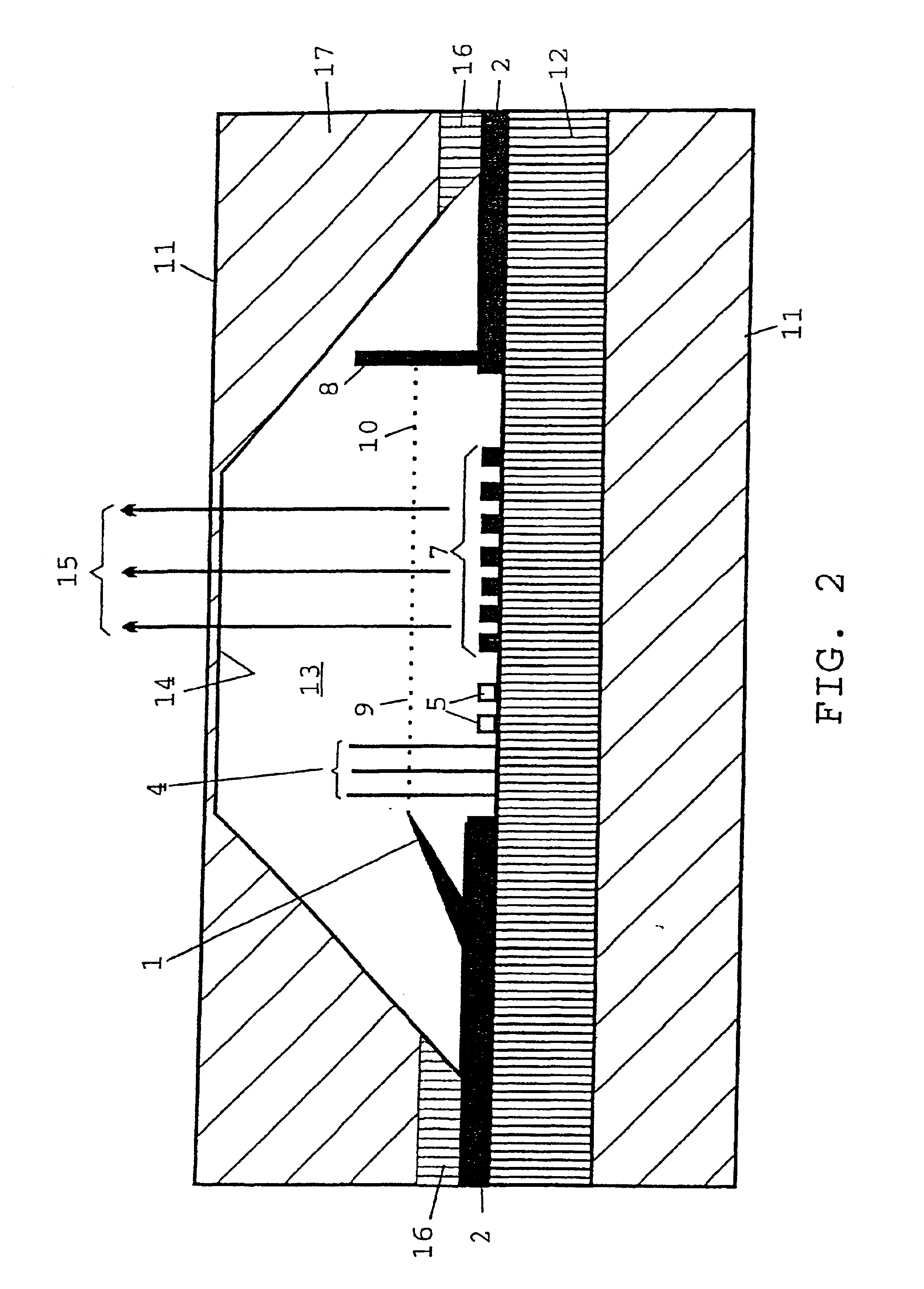
[0007]In exemplary embodiments and / or exemplary methods of the present invention, a high-resolution double-
resist technique and lift-off may be used. The exemplary embodiments and / or exemplary methods may employ new types of technologies to integrate the
electron source, the beam guidance, and the generation of the far-
infrared radiation by the flight of the fast electrons across the
diffraction grating. In this context, given standard sources of up to approximately 20,000 volts accelerating
voltage and an electron beam of 20 μm
diameter over a grating of 100 to 300 μm period, an
infrared radiation in the
far infrared is achieved between 100 μm and one
millimeter wavelength. This radiation may be produced by the image charge, or image
potential energy, which oscillates in response to the electrons flying past the surface profile of the grating. The changing spacing between the charges produces an oscillating
dipole, which may oscillate in coherent fashion along the grating. This ensues due to the
Coulomb interaction of the individual charges on the wires. In this context, the entire electrical field may oscillate coherently in conformance with the individual charges of the rods. In this manner,
electromagnetic radiation is emitted coherently along the entire grating. Its
energy transfer from the electron beam to the
electromagnetic radiation takes place virtually losslessly. The polarization may require a certain
displacement current and, thus, a certain power, but this may be entirely drawn directly from the beam. In exemplary embodiments and / or exemplary methods of the present invention, the oscillating
dipole charge chain may be produced in this manner. In further exemplary embodiments and / or exemplary methods of the present invention, integration of the electron guidance on a chip, and the
direct coupling to the grating having a
high spatial resolution, in the manufacturing process is provided. In further exemplary embodiments and / or exemplary methods of the present invention, micro-
miniaturization may allow for the use of low-energy electrons having energies of between 10 and 1000 eV. Further exemplary embodiments and / or exemplary methods are directed to generating up to 10 kV of electrons on the chip and to implement the guidance by using miniaturized electron-optical components, such as micro-lenses and deflecting elements.
[0008]In further exemplary embodiments and / or exemplary methods of the present invention, when using such high-energy electrons, radiation may also be generated for short wavelengths
ranging from
middle infrared to the visible spectral region. By manufacturing on a common substrate, one ensures
direct coupling to the grating via the
shortest distance to the source, and the manufacturing of the grating and the source on the same chip. In this manner, in further exemplary embodiments and / or exemplary methods, the path of rays of the
electrode configuration, which in a conventional design, may be up to one meter, is reduced to less than 1 mm to 10 mm length. Moreover, a very highly coherent and local
light source may produced, which benefits the temporal and
spatial coherence of the radiation. In exemplary embodiments and / or exemplary methods of the present invention, because the entire electron path is shortened to a greater degree, it may be no longer necessary to use extra-high or high vacuum in the radiation room. It may suffice to cover the
system by a window etched in
silicon using a flipchip bonding technique. This window may be closed by a continuous membrane of
silicon, thereby rendering possible a hollow space. The up to 10 μm high component may be easily accommodated in the hollow space. Into a
silicon wafer of 250 μm thickness, one may etch windows of a few
millimeter diameter, which are sealed by a membrane having a thickness of 10 μm up to 100 μm. This may render a stable mechanical encapsulation of the miniaturized component. In exemplary embodiments and / or exemplary methods of the present invention, it can also be manufactured micromechanically, in
millimeter dimensions. In this context, the required vacuum is approximately 0.01
Torr. In this case, the average free
path length of the electrons in this gas of reduced pressure is as large as the
beam length of the miniaturized component. This can eliminate the need for a pump configuration. The component can be packaged as a ready-made, sealed element and connected. In this manner, a terahertz radiation source may be produced, i.e., a millimeter and submillimeter radiation source on a
semiconductor chip. Through appropriate wave guidance, this radiation source can be linked to further applications.

