Super junction device and corner structure layout design and manufacture process thereof
A super-junction device and layout design technology, which is applied in semiconductor/solid-state device manufacturing, semiconductor devices, electrical components, etc., can solve problems such as insufficient improvement of the overall withstand voltage, and achieve the effect of improving the withstand voltage
- Summary
- Abstract
- Description
- Claims
- Application Information
AI Technical Summary
Problems solved by technology
Method used
Image

Examples
Embodiment Construction
[0045] The present invention will be further described below in conjunction with accompanying drawing:
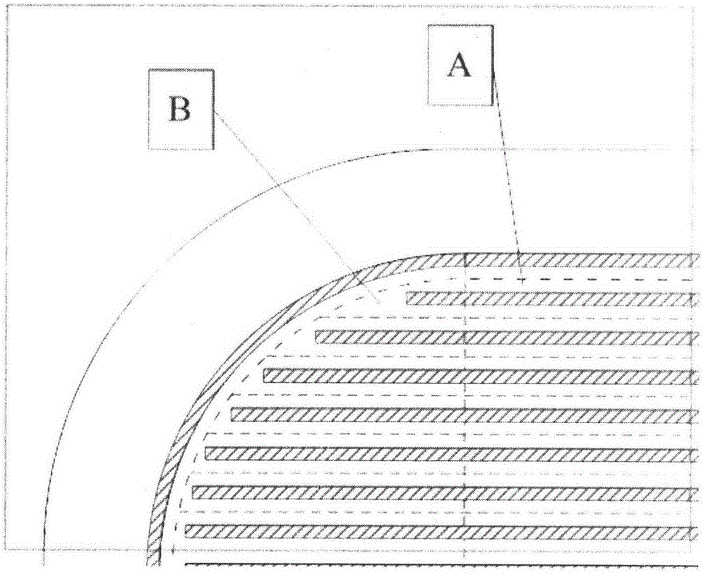
[0046] Such as figure 1 and figure 2 As shown, the corner structure of the superjunction device of the present invention, in the corner region, the boundary of the repeating unit of the cell changes from a straight line (a boundary) to a curve (b boundary), and the doping pattern of the second conductivity type (shading Part) will be optimized and adjusted according to the distance in the vertical direction between the a boundary and the b boundary, so that the area ratio of the first conductivity type doping and the second conductivity type doping in the B' region is the same as that of the ordinary cell region ( figure 1 The ratio in the region A of ) is almost the same, so that the superjunction device can achieve almost the same withstand voltage value as that of the ordinary cell region at the corner.
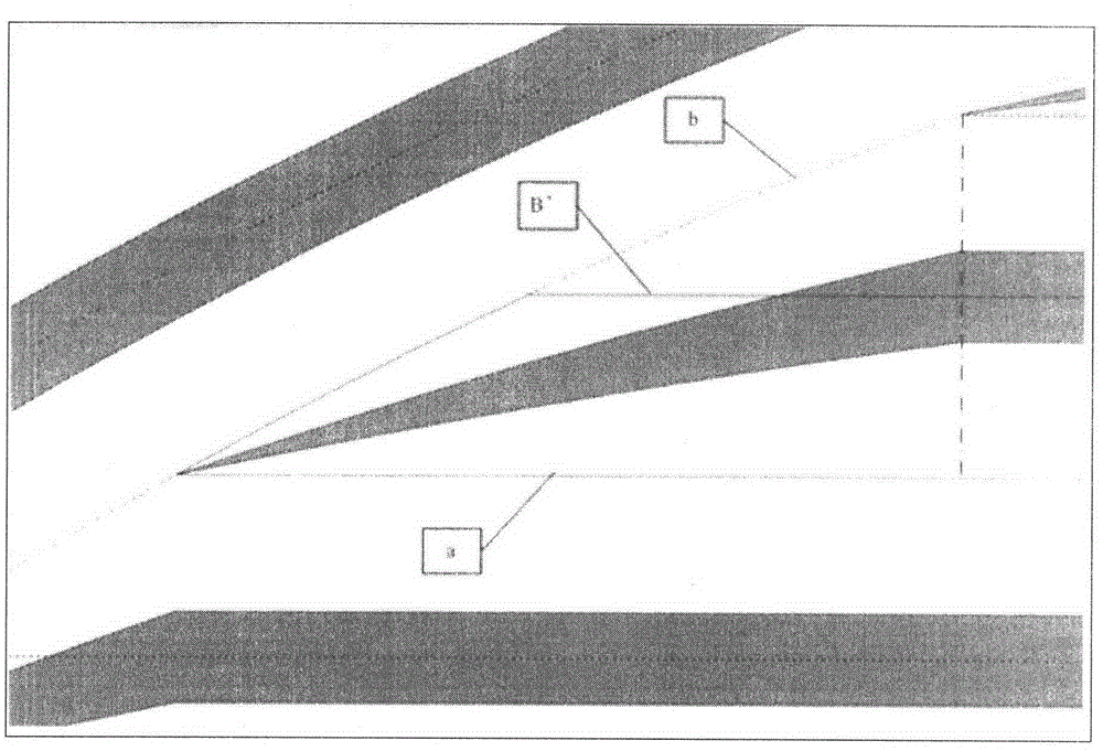
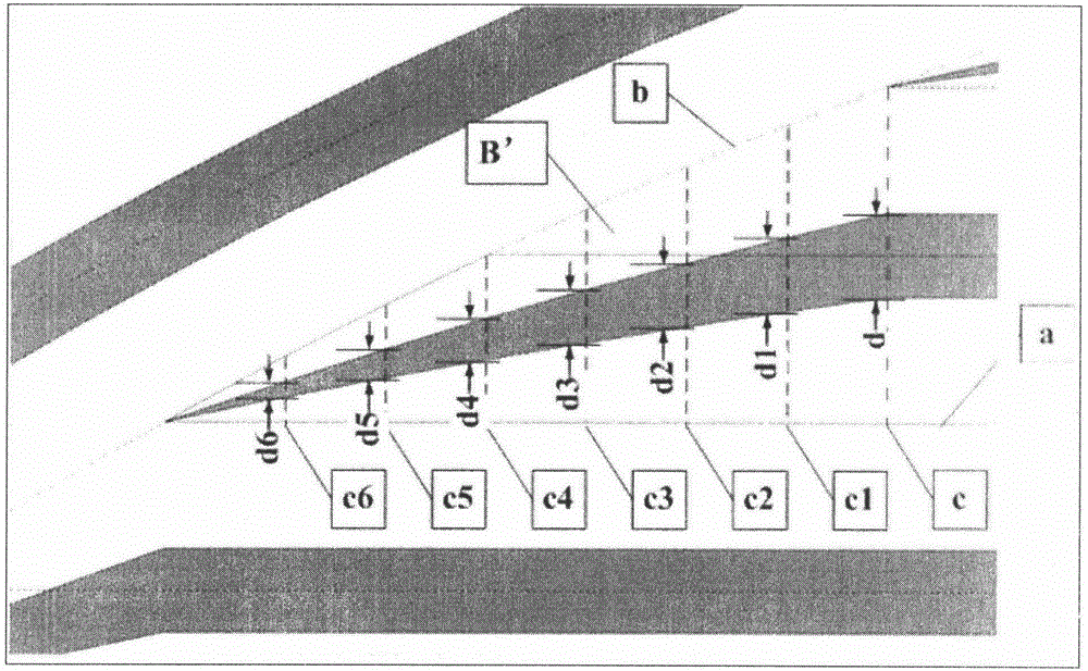
[0047] Such as Figure 3-Figure 5As shown in the layout design...
PUM
 Abstract
Description
Claims
Application Information
 - R&D
- Intellectual Property
- Life Sciences
- Materials
- Tech Scout
- Unparalleled Data Quality
- Higher Quality Content
- 60% Fewer Hallucinations
Browse by: Latest US Patents, China's latest patents, Technical Efficacy Thesaurus, Application Domain, Technology Topic, Popular Technical Reports.
© 2025 PatSnap. All rights reserved.Legal|Privacy policy|Modern Slavery Act Transparency Statement|Sitemap|About US| Contact US: help@patsnap.com