Dual Wavelength Optical Phase Retarder
A technology of optical phase and wavelength delay, applied in optics, optical components, instruments, etc., can solve problems such as inability to use
- Summary
- Abstract
- Description
- Claims
- Application Information
AI Technical Summary
Problems solved by technology
Method used
Image
Examples
Embodiment 1
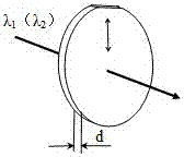
[0039] Such as figure 1 As shown, a dual-wavelength optical phase retarder, which only refers to a single crystal; a single crystal is a parallel flat mirror made of a uniaxial birefringent crystal, and the optical axis of the crystal is parallel to two optical planes; in order to make the single crystal satisfy Retardation required for any two wavelengths, the thickness of a single wafer d Determined by the following two formulas:
[0040]
[0041]
[0042] In the formula lambda 1 and lambda 2 are any two wavelengths, Δn 1 and Δn 2 is the birefringence index corresponding to the two wavelengths of the uniaxial birefringent crystal used, k 1 and k 2 Represents the integer part of the single-chip optical phase retarder to the two-wavelength retardation, that is, the integer multiple of c 1 and c 2 Indicates the fractional part of the retardation of the single-chip optical phase retarder to two wavelengths, that is, (8-m) / 8, where m is an integer greater tha...
Embodiment 2
[0072] Embodiment 2: The similarities between this embodiment and Embodiment 1 will not be repeated, and the difference is:
[0073] 1) The fractional values of the selected two wavelength delays are both 1 / 2, that is c 1 = c 2 =1 / 2;
[0074] 2) Put the relevant data (λ 1 and lambda 2 , Δn 1 and Δn 2 , c 1 and c 2 ) into formula (2), when k 2 When taking a natural number, through numerical calculation, the obtained k 1 The values close to integers and the corresponding single wafer thickness obtained by formula (1) are shown in the table below:
[0075]
[0076] 3) According to the thickness of a single wafer d 1 Value pre-selection principles, choose k 1 =17.0009577 is the preselected value;
[0077] 4) Will k 1 Substitute into formula (1) to get the design value of the thickness of a single wafer d =1.0123mm.
[0078] 5) The fractional part of the retardation of a single chip at 532nm is 180.237°, which belongs to 1 / 2 optical phase retarder;
...
Embodiment 3
[0080] Embodiment 3: The similarities between this embodiment and Embodiment 1 will not be repeated, and the difference is:
[0081]1) The fractional value of the selected two-wavelength retardation c 1 =1 / 4, c 2 =1 / 2.
[0082] 2) Put the relevant data (λ 1 and lambda 2 , Δn 1 and Δn 2 , c 1 and c 2 ) into formula (2), when k 2 When taking a natural number, through numerical calculation, the obtained k 1 The values close to integers and the corresponding single wafer thickness obtained by formula (1) are shown in the table below:
[0083]
[0084] 3) According to the thickness of a single wafer d 1 Value pre-selection principles, choose k 1 =10.0091821 is the preselected value;
[0085] 4) calculated to get k 1 * =10.00459105; will k 1 * Substitute into formula (1) to get the design value of the thickness of a single wafer d =0.5932mm.
[0086] 5) The fractional part of the retardation of a single chip at 532nm is 91.89°, which belongs to 1 / 4 o...
PUM
 Abstract
Description
Claims
Application Information


