Dual-wavelength optical phase delayer

A technology of optical phase and wavelength delay, applied in optics, optical components, instruments, etc., can solve problems such as inability to use

Active Publication Date: 2016-06-22
珠海吉光科技有限公司
View PDF3 Cites 5 Cited by
  • Summary
  • Abstract
  • Description
  • Claims
  • Application Information

AI Technical Summary

Problems solved by technology

[0006] Aiming at the deficiency that the existing birefringent single crystal 1 / 2 and 1 / 4 wave plates are only designed for a specific design wavelength and cannot be used for other wavelengths, the present invention provides a single crystal whose phase retardation for the two wavelengths is equal to 1 / 2, both 1 / 4 and an optical phase retarder with a wavelength of 1 / 2 and another wavelength of 1 / 4

Method used


Image

  • Dual-wavelength optical phase delayer
  • Dual-wavelength optical phase delayer
  • Dual-wavelength optical phase delayer

Examples


Embodiment 1

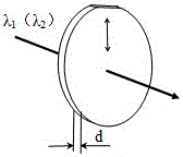
[0039] Such as figure 1 As shown, a dual-wavelength optical phase retarder, which only refers to a single crystal; a single crystal is a parallel flat mirror made of a uniaxial birefringent crystal, and the optical axis of the crystal is parallel to two optical planes; in order to make the single crystal satisfy The retardation required for any two wavelengths, the thickness d of a single crystal is determined by the following two formulas:

[0040]

[0041]

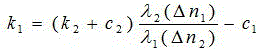
[0042] where λ 1 and lambda 2 are any two wavelengths, Δn 1 and Δn 2 is the birefringence index corresponding to the two wavelengths of the uniaxial birefringent crystal used, k 1 and k 2 Represents the integer part of the single-chip optical phase retarder to the two-wavelength retardation, that is, the integer multiple, c 1 and c 2Indicates the fractional part of the retardation of the single-chip optical phase retarder to two wavelengths, that is, (8-m) / 8, where m is an integer greater than 1-7. Quartz c...

Embodiment 2

[0072] Embodiment 2: The similarities between this embodiment and Embodiment 1 will not be repeated, and the difference is:

[0073] 1) The fractional values ​​of the selected two-wavelength delays are both 1 / 2, that is, c 1 =c 2 =1 / 2;

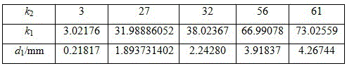
[0074] 2) Put the relevant data (λ 1 and lambda 2 , Δn 1 and Δn 2 、c 1 and c 2 ) into formula (2), when k 2 When taking a natural number, through numerical calculation, the obtained k 1 The values ​​close to integers and the corresponding single wafer thickness obtained by formula (1) are shown in the table below:

[0075]

[0076] 3) According to the single wafer thickness d 1 Value pre-selection principle, choose k 1 =17.0009577 is the preselected value;

[0077] 4) will k 1 Substitute into the formula (1) to obtain the design value of the single wafer thickness d=1.0123mm.

[0078] 5) The fractional part of the retardation of a single chip at 532nm is 180.237°, which belongs to 1 / 2 optical phase retarder;

[0079] The frac...

Embodiment 3

[0080] Embodiment 3: The similarities between this embodiment and Embodiment 1 will not be repeated, and the difference is:

[0081] 1) The fractional value c of the selected two-wavelength retardation 1 =1 / 4,c 2 =1 / 2.

[0082] 2) Put the relevant data (λ 1 and lambda 2 , Δn 1 and Δn 2 、c 1 and c 2 ) into formula (2), when k 2 When taking a natural number, through numerical calculation, the obtained k 1 The values ​​close to integers and the corresponding single wafer thickness obtained by formula (1) are shown in the table below:

[0083]

[0084] 3) According to the single wafer thickness d 1 Value pre-selection principle, choose k 1 =10.0091821 is the preselected value;

[0085] 4) Calculate k 1 * =10.00459105; put k 1 * Substitute into the formula (1) to obtain the design value of the single wafer thickness d=0.5932mm.

[0086] 5) The fractional part of the retardation of a single chip at 532nm is 91.89°, which belongs to 1 / 4 optical phase retarder;

...


PUM


Abstract

The invention provides a dual-wavelength optical phase delayer. A single crystal wafer is a parallel plane mirror made of single-axis birefringence crystal, and the optical axis of the crystal is parallel to two optical planes. In the spectral range of the used single-axis birefringence crystal, the optical phase delayer meeting the requirements that two wavelengths are 1 / 4 or 1 / 2 or one wavelength is 1 / 4 and the other wavelength is 1 / 2 phase retardation is manufactured by using the single birefringence crystal wafer according to the concrete application requirements. The thickness conditions of the single crystal wafer which are necessarily met and the design steps based on the conditions are given: 1) the designed wavelengths lambda<1> and lambda<2> and the fractional values c<1> and c<2> of phase retardation are determined; 2) the used birefringence crystal is determined, and birefringence deltan<1> and deltan<2> are obtained according to the refraction index dispersion formula of the crystal; 3) when k<2> is natural numbers 1,2,3,......, the corresponding values of series k<1> are obtained through numerical calculation; and 4) the integers close to k<1> are represented by k<10>, and when the value of a certain k<1> meets the expression ||<=0.005, the thickness of the single crystal wafer is determined by the value of k<1>.

Description

technical field [0001] The invention belongs to the technical field of optical phase retarders in polarization optics, and relates to a dual-wavelength optical phase retarder and a design method. Background technique [0002] Polarization technology has a wide range of applications in optical fiber communication, space optical communication, optical measurement (including ellipsometry), and laser processing. The basis of polarized light technology is various types of polarized light including linear polarization, circular polarization and elliptical polarization. [0003] Circularly polarized light and elliptically polarized light are produced by linearly polarized light passing through an optical phase retarder. When the fast axis of the 1 / 4 phase retarder is at an angle of 45° to the vibration direction of the incident linearly polarized light, the outgoing light is circularly polarized light; when the fast axis of the 1 / 4 phase retarder is at an angle to the vibration di...

Claims


Application Information

Patent Timeline
Patent Type & Authority Applications(China)
IPC IPC(8): G02B5/30
CPCG02B5/3083
Inventor 吴闻迪吴福全
Owner 珠海吉光科技有限公司
Why Eureka
Try Eureka