BeZnOS compound semiconductor material as well as preparation method and application thereof

A semiconductor and compound technology, applied in the field of BeZnOS compound semiconductor materials, can solve problems such as the preparation of BeZnOS quaternary compound semiconductor materials that have not yet been seen, and achieve the effect of improving electron and hole characteristics, simple equipment and operation process, and good crystallinity.

Inactive Publication Date: 2016-07-06
HUBEI UNIV
View PDF3 Cites 18 Cited by
  • Summary
  • Abstract
  • Description
  • Claims
  • Application Information

AI Technical Summary

Problems solved by technology

At present, there are some reports on BeZnO and ZnOS semiconductor materials, but there is no report on the preparation of BeZnOS quaternary compound semiconductor materials.

Method used


Image

  • BeZnOS compound semiconductor material as well as preparation method and application thereof
  • BeZnOS compound semiconductor material as well as preparation method and application thereof
  • BeZnOS compound semiconductor material as well as preparation method and application thereof

Examples


Embodiment 1

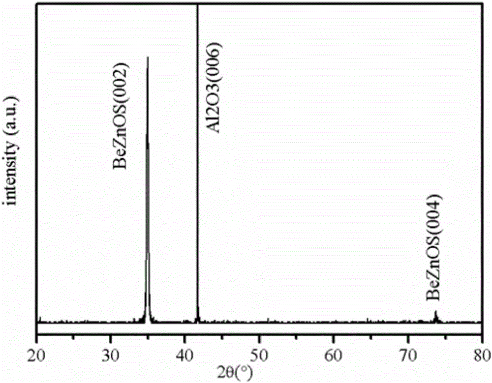
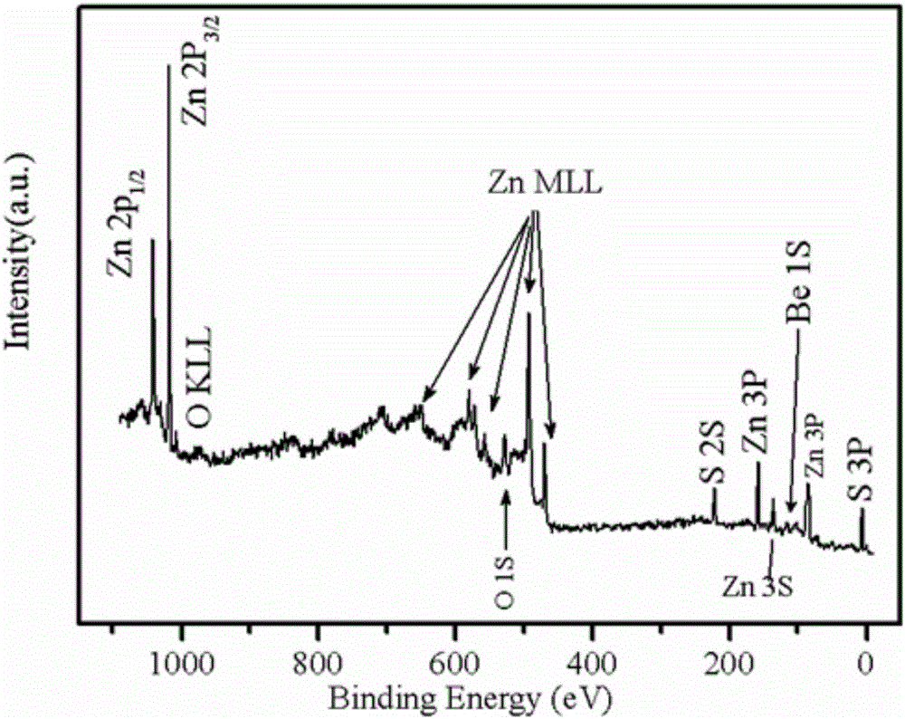
[0033] Weigh 18.5193 g of ZnS powder and 2.5012 g of BeO powder according to the molar ratio of ZnS:BeO=95:5, add 13 g of deionized water and ball mill for 4 hours after mixing, and then vacuum dry at 110°C. The dried powder is mixed with 2 g of ethanol, fully ground and stirred, and then compressed into a circular green sheet with a diameter of 27.5 mm and a thickness of 2 mm. The green sheet is placed in a crucible and placed in a vacuum tube furnace, and powder with the same composition (5.0000 g) and high-purity sulfur powder (1.1000 g) are placed around it. The vacuum tube furnace is evacuated to 0.1Pa and then high-purity argon is introduced. In a protective atmosphere, the tube furnace was heated to 1300° C. and kept for 2 hours, and then naturally cooled to room temperature to obtain the desired ceramic target. Using this ceramic target as a laser ablation target, it was put into a vacuum chamber together with a substrate that was ultrasonically cleaned with acetone, a...

Embodiment 2

[0035] Weigh 16.5700 grams of ZnS powder and 7.5036 grams of BeO powder according to the molar ratio of ZnS:BeO=85:15, add 12 grams of deionized water and ball mill for 4 hours after mixing, and then vacuum dry at 110°C. The dried powder is mixed with 2 g of ethanol, fully ground and stirred, and then compressed into a circular green sheet with a diameter of 27.5 mm and a thickness of 2.5 mm. The green sheet is put into a crucible and placed in a vacuum tube furnace, and the same powder and high-purity sulfur powder are placed around it. The vacuum tube furnace is evacuated to 0.1Pa and then high-purity argon is introduced. In a protective atmosphere, the tube furnace was heated to 1100° C. and kept for 5 hours, and then naturally cooled to room temperature to obtain the desired ceramic target. Use this ceramic target as a laser ablation target, and put it into a vacuum chamber together with a substrate that has been ultrasonically cleaned with acetone, absolute ethanol and de...

Embodiment 3

[0037] Weigh 17.9345 grams of ZnS powder and 6.0216 grams of BeO powder according to the molar ratio of ZnS:BeO=92:8, add 24 grams of deionized water and ball mill for 4 hours after mixing, and then vacuum dry at 110°C. The dried powder is mixed with 2 g of ethanol, fully ground and stirred, and then compressed into a circular green sheet with a diameter of 27.5 mm and a thickness of 3 mm. The green sheet is put into a crucible and placed in a vacuum tube furnace, and the same powder and high-purity sulfur powder are placed around it. The vacuum tube furnace is evacuated to 0.1Pa and then high-purity argon is introduced. In a protective atmosphere, the tube furnace was heated to 750° C. and kept for 6 hours, and then naturally cooled to room temperature to obtain the desired ceramic target. Use this ceramic target as a laser ablation target, and put it into a vacuum chamber together with a substrate that has been ultrasonically cleaned with acetone, absolute ethanol and deioni...


PUM

PropertyMeasurementUnit
thicknessaaaaaaaaaa
band gapaaaaaaaaaa
particle sizeaaaaaaaaaa

Abstract

The invention belongs to the technical field of semiconductor optoelectronic materials, and in particular relates to a BeZnOS compound semiconductor material, its preparation method and application. The BeZnOS material provided by the present invention is a quaternary compound semiconductor material obtained by solid solution of BeO and ZnS in a certain proportion. Through the synergistic effect of compound substitution of Be and S, not only can the bandgap of ZnO be adjusted more freely, but also play a role Increase the solubility of the substituting elements Be and S in ZnO and eliminate the effect of mutual restraint between the band gap of the solid solution and the adjustment of the lattice constant. The BeZnOS quaternary compound is a wide bandgap semiconductor with freely adjustable bandgap, and can be used for light-emitting devices or photodetection devices in ultraviolet to solar blind regions. The BeZnOS compound semiconductor material provided by the invention can be grown by various methods such as pulse laser deposition, magnetron sputtering, electron beam evaporation, etc., and the equipment and operation process are simple. The BeZnOS single crystal thin film material provided by the invention is successfully synthesized for the first time in the world, and has very important significance for the development of ZnO-based optoelectronic devices with adjustable wavelength.

Description

Technical field [0001] The invention belongs to the technical field of semiconductor optoelectronic materials, and specifically relates to a BeZnOS compound semiconductor material, a preparation method and application thereof. Background technique [0002] The third-generation wide-gap semiconductor ZnO has a forbidden band width of 3.3eV and an exciton binding energy of 60meV. It has potential wide-ranging applications in blue light, ultraviolet light emission, and photodetection. In order to achieve device applications, it is often necessary to substitute ZnO for doping to adjust its energy band. For example, the BeZnO ternary compound is obtained by partially replacing Zn with Be to obtain a wider band gap. BeZnO is formed by solid solution of ZnO and BeO according to a certain component ratio. BeO and ZnO have the same hexagonal structure. The band gap of BeO (10.8eV) is much larger than that of ZnO. Therefore, only a small amount of Be is dissolved in ZnO. While expanding ...

Claims


Application Information

Patent Timeline
Patent Type & Authority Applications(China)
IPC IPC(8): C23C14/06C23C14/28
CPCC23C14/06C23C14/28
Inventor 何云斌张武忠黎明锴程海玲唐志武
Owner HUBEI UNIV
Why Eureka
Try Eureka