A kind of cdznos quaternary zno alloy semiconductor material and preparation method thereof

A semiconductor and alloy technology, applied in the field of semiconductor optoelectronic material preparation, can solve problems such as CdZnOS quaternary ZnO alloy semiconductor materials that have not yet been seen, and achieve the effects of easy control, simple equipment and operation process

Active Publication Date: 2016-08-24
HUBEI UNIV
View PDF5 Cites 0 Cited by
  • Summary
  • Abstract
  • Description
  • Claims
  • Application Information

AI Technical Summary

Problems solved by technology

[0003] At present, there are some reports on CdZnO and ZnOS semiconductor materials, but there is no report on Cd and S co-doped into ZnO to prepare CdZnOS quaternary ZnO alloy semiconductor materials.

Method used


Image

  • A kind of cdznos quaternary zno alloy semiconductor material and preparation method thereof
  • A kind of cdznos quaternary zno alloy semiconductor material and preparation method thereof
  • A kind of cdznos quaternary zno alloy semiconductor material and preparation method thereof

Examples


Embodiment 1

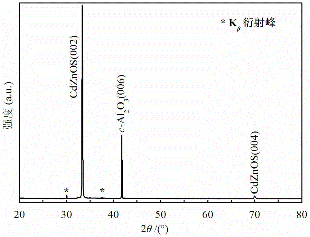
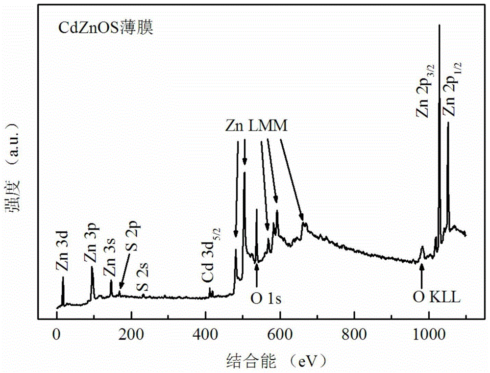
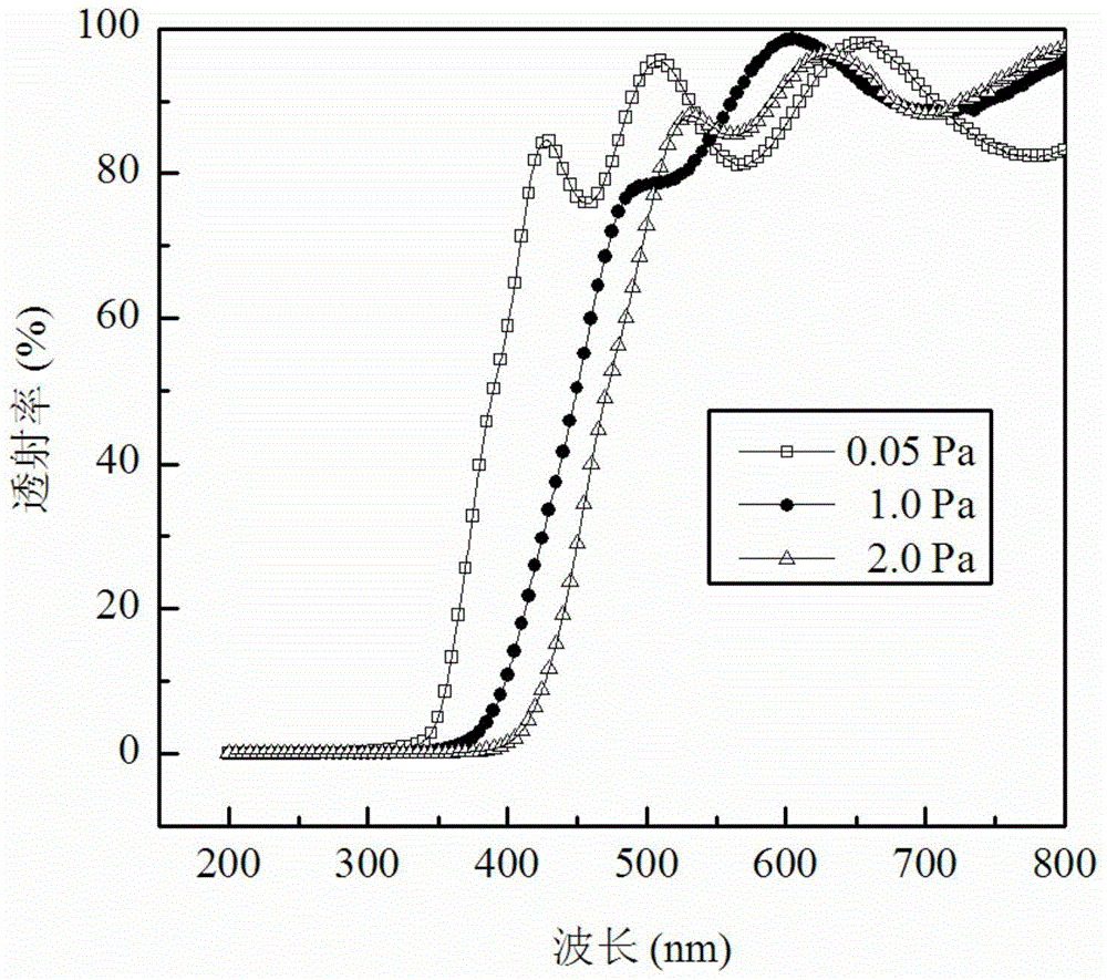
[0028] Weigh 21.8880 g of ZnS powder and 8.1120 g of CdO powder (molar ratio ZnS:CdO=80:20) and place them in a ball mill jar, add 18 mL of deionized water and ball mill for 4 hours, and then dry them in a vacuum oven at 100°C and 0.1Pa 6 hours. The dried powder was added with 1.8 mL of deionized water to fully grind and stir, and then pressed into a circular green sheet with a diameter of 21 mm and a thickness of 2 mm. The billets are placed in a crucible and placed in a vacuum tube furnace, surrounded by powders of the same composition and high-purity sulfur powder. The vacuum tube furnace was evacuated to 0.1 Pa, and then high-purity argon was introduced. Under a protective atmosphere, the temperature of the tube furnace was raised to 600° C. and kept for 3 hours, and then naturally cooled to room temperature to obtain the desired ceramic material. The ceramic material is used as the laser ablation target, and the c-plane sapphire is used as the substrate. The substrate ...

Embodiment 2

[0031] Weigh 21.8880 g of ZnS powder and 8.1120 g of CdO powder (molar ratio ZnS:CdO=80:20) and place them in a ball mill jar, add 18 mL of deionized water and ball mill for 4 hours, and then dry them in a vacuum oven at 100°C and 0.1Pa 6 hours. The dried powder was added with 1.8 mL of deionized water to fully grind and stir, and then pressed into a circular blank with a diameter of 21 mm and a thickness of 3 mm. The green sheet is placed in a crucible and placed in a vacuum tube furnace, and the powder and sulfur powder with the same composition are placed around it. The vacuum tube furnace was evacuated to 0.1 Pa, and then high-purity argon was introduced. Under a protective atmosphere, the temperature of the tube furnace was raised to 600° C. and kept for 3 hours, and then naturally cooled to room temperature to obtain the desired ceramic material. The ceramic material is used as the laser ablation target, and the c-plane sapphire is used as the substrate. The substrate...

Embodiment 3

[0034]Weigh 13.9143 grams of ZnS powder and 1.0857 grams of CdO powder (molar ratio ZnS:CdO=95:5) and place them in a ball mill jar, add 9 mL of deionized water and ball mill for 4 hours, and then dry them in a vacuum oven at 100°C and 0.1Pa 6 hours. The dried powder was added with 0.9 mL of deionized water to fully grind and stir, and then pressed into a circular blank with a diameter of 21 mm and a thickness of 2 mm. The billets are placed in a crucible and placed in a vacuum tube furnace, surrounded by powders of the same composition and high-purity sulfur powder. The vacuum tube furnace was evacuated to 0.1 Pa, and then high-purity argon was introduced. Under a protective atmosphere, the temperature of the tube furnace was raised to 700° C. and kept for 3 hours, and then naturally cooled to room temperature to obtain the desired ceramic material. The ceramic material is used as the laser ablation target, and the c-plane sapphire is used as the substrate. The substrate w...


PUM

PropertyMeasurementUnit
thicknessaaaaaaaaaa
band gapaaaaaaaaaa

Abstract

The invention discloses a CdZnOS quaternary ZnO alloy semiconductor material and a preparation method thereof. The preparation method comprises the following steps: enabling Cd and S to be simultaneously doped with ZnO, and adjusting the ratio of Cd to Zn to O to S in CdZnOS to form the brand-new CdZnOS quaternary ZnO alloy semiconductor material, wherein a wide bandgap semiconductor with a bandgap adjustable within a relatively wide range is obtained and can be used for luminescent devices or light detection devices. A reported CdZnOS single-crystal material is successfully synthesized for the first time in the world, and the preparation of the CdZnOS quaternary ZnO alloy semiconductor is of great significance on development of wavelength-adjustable photoelectric devices; the CdZnOS quaternary ZnO alloy semiconductor material can grow by various methods of conventional pulsed laser deposition, magnetron sputtering, electron beam evaporation and the like; equipment and the operation process are simple, and the control is easy.

Description

technical field [0001] The invention belongs to the field of semiconductor photoelectric material preparation, in particular to a CdZnOS quaternary ZnO alloy semiconductor material and a preparation method thereof. Background technique [0002] The third-generation wide bandgap semiconductor ZnO has a bandgap width of about 3.3eV and an exciton binding energy of 60 meV, and has a very wide range of uses in optoelectronic devices. Doping ZnO to adjust its energy band can broaden its wavelength range and realize a wider range of device applications. For example, in ZnO-based semiconductor materials, Cd is used to replace Zn, and CdZnO, which is a solid solution of ZnO and CdO in a certain composition, has a narrower forbidden band than ZnO. Experiments have proved that the band gap of CdZnO can be adjusted monotonously and continuously from 3.3eV to 1.8eV by changing the content of Cd. On the other hand, in addition to replacing Zn with cations 2+ , can also replace the O o...

Claims


Application Information

Patent Timeline
Patent Type & Authority Patents(China)
IPC IPC(8): C23C14/28C23C14/08
CPCC23C14/086C23C14/28
Inventor 何云斌黎明锴郑丽兰
Owner HUBEI UNIV
Why Eureka
Try Eureka