Photodiode and manufacturing method thereof, X-ray detection substrate and manufacturing method thereof

A technology for photodiodes and detection substrates, applied in circuits, electrical components, electrical solid devices, etc., can solve the problems of fixed doping concentration, inability to achieve special regionalization of doping, and inability to control precisely

Active Publication Date: 2017-10-17
BOE TECH GRP CO LTD
View PDF4 Cites 0 Cited by
  • Summary
  • Abstract
  • Description
  • Claims
  • Application Information

AI Technical Summary

Problems solved by technology

The PIN preparation method of the indirect X-ray detection substrate mainly adopts PECVD technology, through different process gases (such as: SiH 4 , NH 3 , N 2 O.PH 3 、H 2 、B 2 h 6 etc.) can form PIN devices conveniently and quickly at the same time, but its disadvantage is that the doping concentration is relatively fixed, cannot be precisely controlled, and cannot achieve special regionalized doping

Method used


Image

  • Photodiode and manufacturing method thereof, X-ray detection substrate and manufacturing method thereof
  • Photodiode and manufacturing method thereof, X-ray detection substrate and manufacturing method thereof
  • Photodiode and manufacturing method thereof, X-ray detection substrate and manufacturing method thereof

Examples


Embodiment Construction

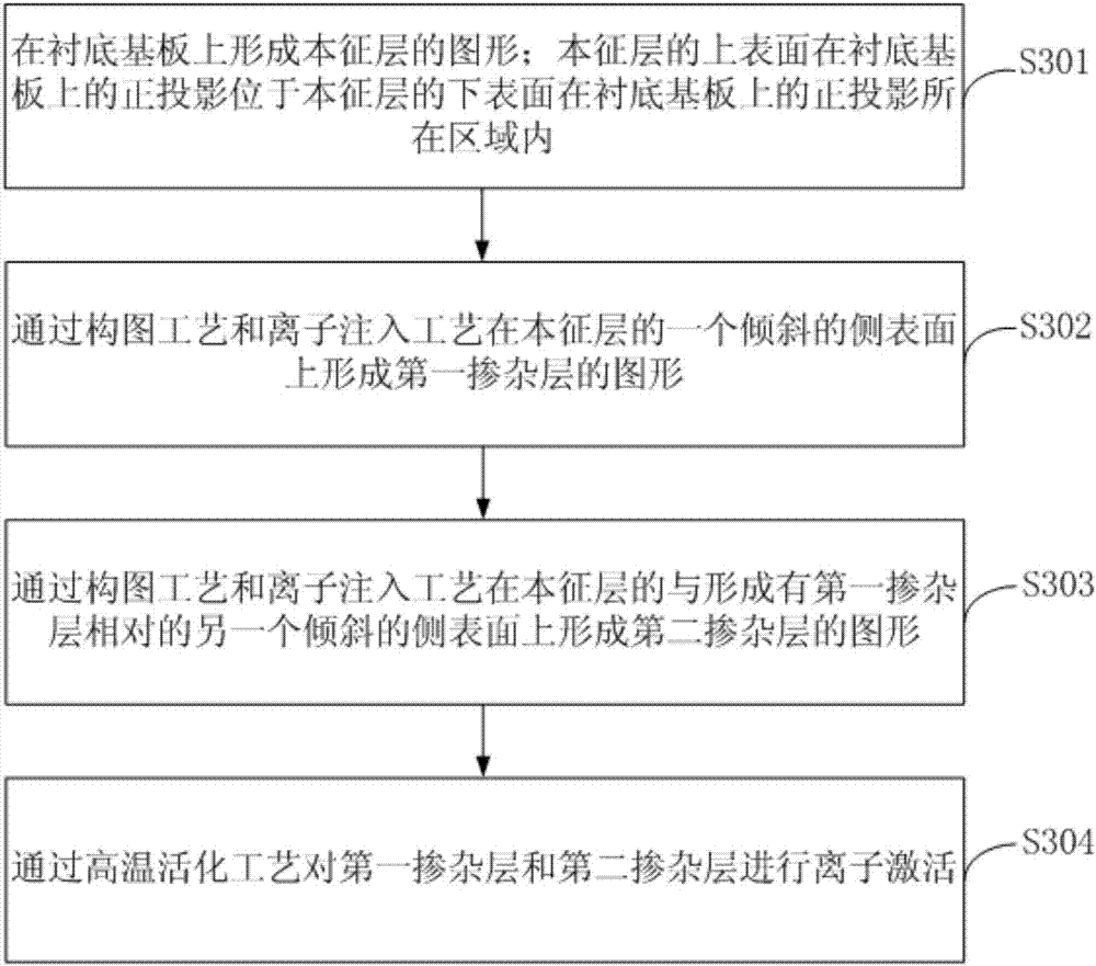
[0061] Specific implementations of the photodiode and its manufacturing method, the X-ray detection substrate and its manufacturing method provided by the embodiments of the present invention will be described in detail below with reference to the accompanying drawings.

[0062] Wherein, the thickness and shape of each film layer in the drawings do not reflect the real ratio of the PIN photodiode and the X-ray detection substrate, and the purpose is only to illustrate the content of the present invention.

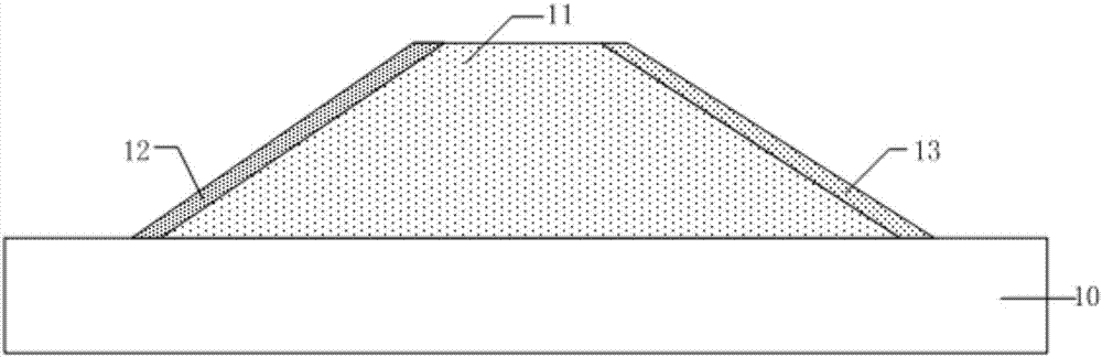
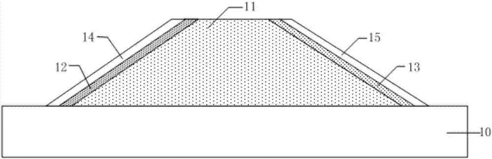
[0063] An embodiment of the present invention provides a PIN photodiode, such as figure 1 As shown, it includes: a base substrate 10, and an intrinsic layer 11, a first doped layer 12 and a second doped layer 13 located on the base substrate 10;

[0064] The orthographic projection of the upper surface of the intrinsic layer 11 on the base substrate 10 is located in the area where the orthographic projection of the lower surface of the intrinsic layer 11 on the base substra...


PUM


Abstract

The invention discloses a photodiode and a manufacturing method thereof, an X-ray detection substrate and the manufacturing method of the X-ray detection substrate. The photodiode comprises a substrate, an intrinsic layer, a first doped layer and a second doped layer, wherein the intrinsic layer, the first doped layer and the second doped layer are located on the substrate; the orthographic projection, on the substrate, of the upper surface of the intrinsic layer is located in a region, in which the orthographic projection on the substrate is located, on the lower surface of the intrinsic layer; and the first doped layer and the second doped layer are located on two opposite inclined side surfaces of the intrinsic layer respectively. According to the photodiode structure disclosed by the embodiment of the invention, the first doped layer and the second doped layer are located on the two opposite inclined side surfaces of the intrinsic layer respectively; and doping can be carried out in an ion implantation manner in the manufacturing process, so that the doping concentration can be accurately controlled; effective control on the performance of the photodiode is achieved; the effective light interception area of the photodiode can be increased through the arranged inclined side surfaces; collected photon-generated carriers are large in quantity; and the generated signal intensity is high.

Description

technical field [0001] The invention relates to the field of display technology, in particular to a photodiode and a manufacturing method thereof, an X-ray detection substrate and a manufacturing method thereof. Background technique [0002] X-ray inspection is widely used in medical, safety, non-destructive testing, scientific research and other fields, and it is increasingly playing an important role in the national economy and people's livelihood. At present, in actual use, X-ray detection generally uses film photography. The imaging quality of X-ray film photography is high, and it can correctly provide reliable information on the physical appearance and defects of the tested piece. However, it has the disadvantages of complicated operation process, high operating cost, difficult preservation of results, inconvenient query and portability, and easy access to the eyes of reviewers. Disadvantages such as damage by strong light. In order to solve the above problems, X-ray ...

Claims


Application Information

Patent Timeline
Patent Type & Authority Patents(China)
IPC IPC(8): H01L31/0352H01L31/117H01L27/146H01L31/20
CPCH01L27/14659H01L31/035281H01L31/117H01L31/202
Inventor 赵磊田彪
Owner BOE TECH GRP CO LTD
Why Eureka
Try Eureka