Supercharge Your Innovation With Domain-Expert AI Agents!

Optical surface profile scanning system

A surface profile and scanning system technology, applied in the direction of optical devices, measuring devices, instruments, etc., can solve the problems of probe wear or damage, increased use cost, probe scratches, etc., and achieve short measurement time and good image quality , the effect of easy operation

Inactive Publication Date: 2016-07-13
METAL INDS RES & DEV CENT
View PDF6 Cites 2 Cited by
  • Summary
  • Abstract
  • Description
  • Claims
  • Application Information

AI Technical Summary

Problems solved by technology

However, if the surface hardness of the object to be measured is lower than that of the probe, or the force applied by the probe to the surface of the object to be measured is too large, the probe will often scratch the surface of the object to be measured, causing troubles in use; It will also be worn or damaged during measurement, so the probe is a consumable, and frequent replacement of the probe will also increase the cost of use

Method used


Image

  • Optical surface profile scanning system
  • Optical surface profile scanning system
  • Optical surface profile scanning system

Examples


Embodiment Construction

[0038] The technical means adopted by the present invention to achieve the intended invention purpose are further described below in conjunction with the drawings and preferred embodiments of the present invention.

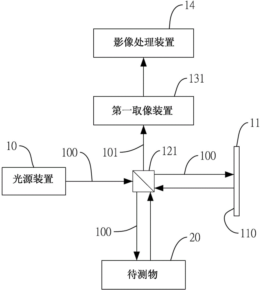
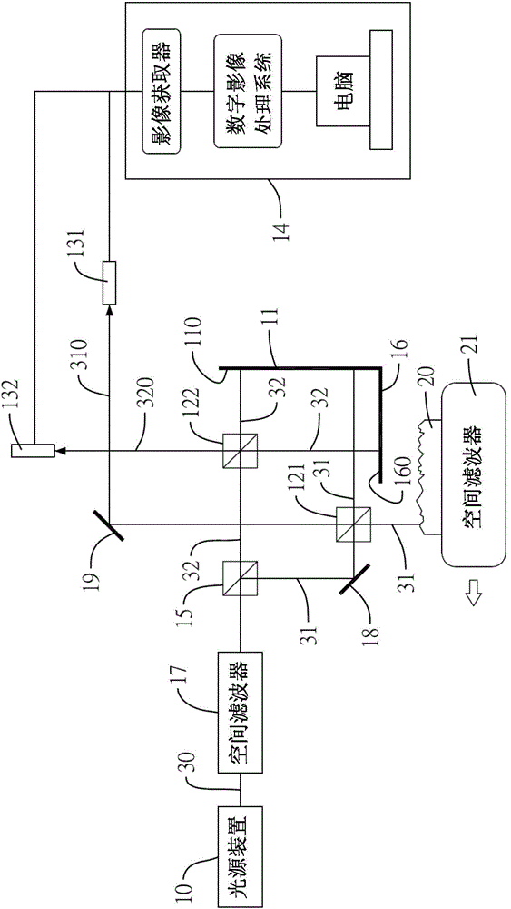
[0039] Please refer to figure 1 , The optical surface profile scanning system of the present invention mainly includes a light source device 10 , an interference mirror 11 , a first beam splitter 121 , a first imaging device 131 and an image processing device 14 .

[0040] The light source device 10 can be a He-Ne laser device or a LED device for emitting a detection beam 100 . The interference reflector 11 has an interference reflective surface 110, and the interference reflective surface 110 can face the light source device 10 for reflecting light beams.

[0041] The first spectroscope 121 is arranged in the optical path of the detection beam 100, and the detection beam 100 is simultaneously projected onto the surface of an object to be tested 20 and the interf...


PUM


Abstract

The invention relates to an optical surface profile scanning system, which comprises a light source device, an interference reflector, a first spectroscope and an image processing device. The light source device emits detection light beams. The first spectroscope simultaneously projects the detection light beams onto the surface of a to-be-detected object and the detection light beams are reflected by the first interference reflector respectively. After the detection light beams, projected onto the surface of the to-be-detected object and reflected by the first interference reflector, interfere with one another in the first spectroscope, the first spectroscope projects the surface interference image of the to-be-detected object to a first image sampling device. The image processing device receives the surface interference image of the to-be-detected object through the first image sampling device and then subtracts the surface interference image of the to-be-detected object by a reference interference image to obtain a difference image. Referring to the difference image, the surface profile of the to-be-detected object is established. According to the technical scheme of the invention, the surface profile of the to-be-detected object is measured in the non-contact manner, so that the to-be-detected object is free from being scratched. Meanwhile, no probe is adopted, so that the cost of the probe is saved.

Description

technical field [0001] The invention relates to an optical surface profile scanning system, which projects light beams to detect the profile of a surface to be measured. Background technique [0002] The probe-type measuring device is a device for measuring the surface profile of an object to be measured. The probe-type measuring device mainly includes a probe and a mobile platform, and an object to be measured is arranged on the mobile platform. When performing measurement operations, the probe directly contacts the surface of the object to be measured, and at the same time controls the mobile platform to move relative to the probe, so that the probe slides along a track on the surface of the object to be measured, and the probe is connected to the surface of the object to be measured. A controller of the needle detects the working parameters of the probe (such as the magnitude of the force) to determine the surface profile of the object to be tested. However, if the surfa...

Claims


Application Information

Patent Timeline
IPC IPC(8): G01B11/24
Inventor 林原志侯博勋
Owner METAL INDS RES & DEV CENT
Features
  • R&D
  • Intellectual Property
  • Life Sciences
  • Materials
  • Tech Scout
  • Unparalleled Data Quality
  • Higher Quality Content
  • 60% Fewer Hallucinations
Learn More