
MOS structure used for packaging level reliability test and manufacturing method thereof

A MOS structure and reliability technology, applied in semiconductor/solid-state device testing/measurement, electrical components, electrical solid-state devices, etc., can solve the problem of unsatisfied resonance conditions, and achieve the effect of avoiding resonance

Inactive Publication Date: 2016-07-20
SHANGHAI HUALI MICROELECTRONICS CORP
View PDF7 Cites 3 Cited by
  • Summary
  • Abstract
  • Description
  • Claims
  • Application Information

AI Technical Summary

Problems solved by technology

[0006] The technical problem to be solved by the present invention is to change the capacitance value of the output capacitor of the packaging-level MOS structure, so that the conditions for resonance with the power frequency cannot be satisfied, and to achieve the ultimate goal of avoiding resonance during reliability testing

Method used


Image

  • MOS structure used for packaging level reliability test and manufacturing method thereof
  • MOS structure used for packaging level reliability test and manufacturing method thereof
  • MOS structure used for packaging level reliability test and manufacturing method thereof

Examples


Embodiment Construction

[0032] In order to make the content of the present invention clearer and easier to understand, the content of the present invention will be further described below in conjunction with the accompanying drawings. Of course, the present invention is not limited to this specific embodiment, and general replacements known to those skilled in the art are also covered within the protection scope of the present invention.

[0033] Secondly, the present invention is described in detail by means of schematic diagrams. When describing the examples of the present invention in detail, for the convenience of explanation, the schematic diagrams are not partially enlarged according to the general scale, which should not be used as a limitation of the present invention.

[0034] Embodiments of the present invention will be further described below in conjunction with the accompanying drawings.

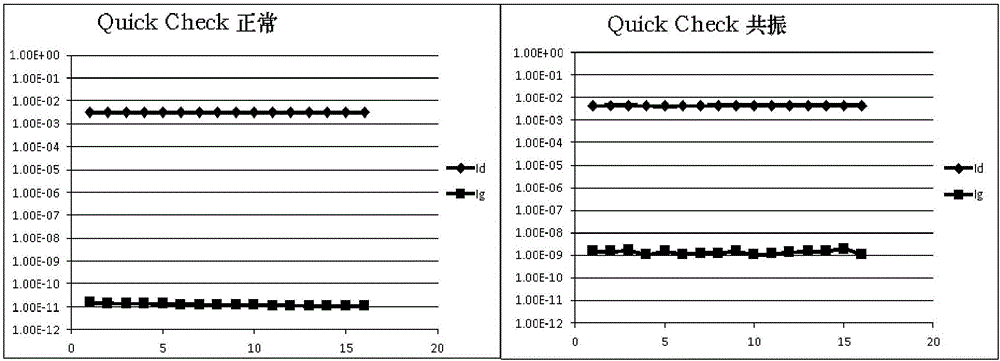
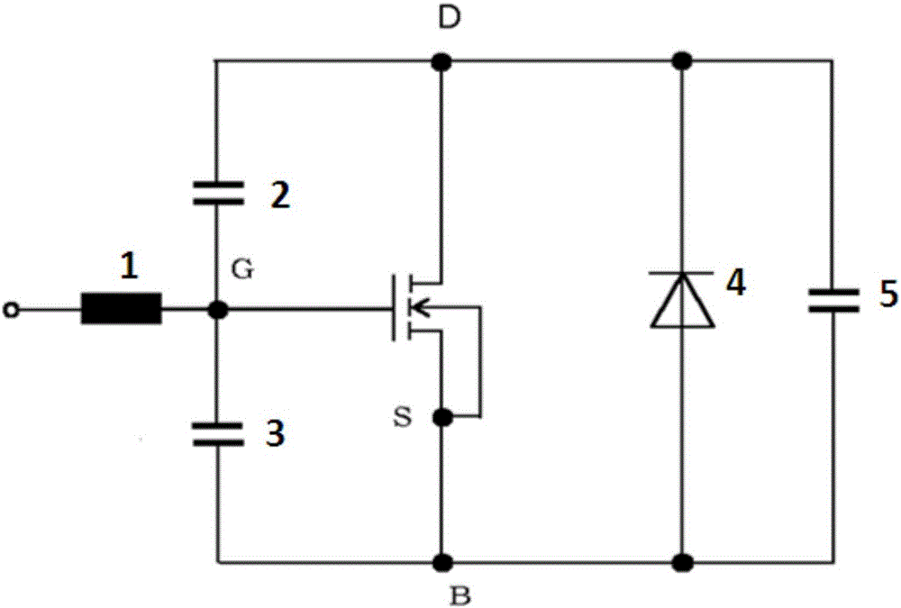
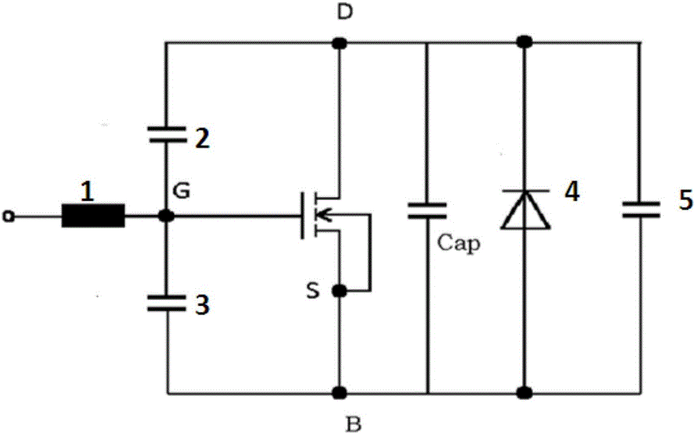
[0035] In this embodiment, a packaged NMOS is used as a package-level MOS structure for reliability ...


PUM


Abstract

The invention provides a MOS structure used for a packaging level reliability test. An equivalent circuit is characterized in that a grid electrode, a drain electrode, a source electrode and a substrate are connection points; the source electrode and the substrate are connected so as to be served as an equipotential point; a capacitor is added between the drain electrode and the substrate so that the capacitor is parallel to an output capacitor CDS of a tested MOS. The invention also provides a manufacturing method of the MOS structure used for the packaging level reliability test. A process of an original MOS structure is used. The capacitor is added in the tested MOS structure. An active region is taken as a lower pole plate. A gate oxide layer is used as a medium. A polycrystal is taken as an upper pole plate. A contact hole and metal in the original MOS process are used to make the upper pole plate of the capacitor be connected with the drain electrode of the MOS structure, and the lower pole plate be connected with the substrate of the MOS structure. Parallel connection with the original output capacitor CDS of the MOS structure is realized so as to change a capacitance value of an actual output capacitance, which means that an impressed frequency is changed and a condition of generating resonance with a power frequency (50Hz) can not be satisfied. Therefore, a final purpose of avoiding generating the resonance during the reliability test is reached.

Description

technical field [0001] The invention relates to the technical field of integrated circuits, in particular to a MOS structure used for packaging level reliability testing and a preparation method thereof. Background technique [0002] In the prior art, before performing the reliability test of the package-level device, it is necessary to perform a QuickCheck to determine whether the initial parameters of the device under test are normal. Usually QuickCheck needs to measure the leakage current of the drain Id and gate Ig of the device under test, and also rejects the open or short failures of the device under test. [0003] In actual operation, QuickCheck will drift in the measured value due to resonance in the test, and the results are as follows figure 1 shown. figure 1 The left part in the middle is the normal QuickCheck result, indicating that the device under test is normal, and the right part is the QuickCheck result after resonance occurs. Obviously, the values ​​​​of...

Claims


Application Information

Patent Timeline
Patent Type & Authority Applications(China)
IPC IPC(8): H01L23/544H01L29/06H01L21/66
CPCH01L23/544H01L22/14H01L22/30H01L29/0603
Inventor 王炯周柯尹彬锋
Owner SHANGHAI HUALI MICROELECTRONICS CORP
Learn More