
Semiconductor process control method and semiconductor process control system

A process control and semiconductor technology, applied in the direction of comprehensive factory control, comprehensive factory control, electrical program control, etc., can solve the problems of reducing the transmission efficiency of damaged materials, reducing the stability of machine transmission, and prone to error operations, etc., to avoid The effect of unstable machine transmission, avoiding manual participation in the process, and saving transmission time

Active Publication Date: 2018-11-06
BEIJING NAURA MICROELECTRONICS EQUIP CO LTD
View PDF6 Cites 0 Cited by
  • Summary
  • Abstract
  • Description
  • Claims
  • Application Information

AI Technical Summary

Problems solved by technology

[0004] When using manual transmission to the designated material chamber, it is also necessary to manually set the process modules on the transmission path to the task-available state, and step by step the damaged materials stagnant in each chamber according to the actual situation inside the machine. The material is transported to the designated material chamber, and the operator observes the transmission situation inside the machine while operating the software, which wastes a lot of time and reduces the transmission efficiency of damaged materials, and due to manual participation, it is prone to misoperation, reducing the Stability of machine transmission

Method used


Image

  • Semiconductor process control method and semiconductor process control system
  • Semiconductor process control method and semiconductor process control system
  • Semiconductor process control method and semiconductor process control system

Examples


Embodiment Construction

[0028] Embodiments of the present invention are described in detail below, examples of which are shown in the drawings, wherein the same or similar reference numerals designate the same or similar elements or elements having the same or similar functions throughout. The embodiments described below by referring to the figures are exemplary and are intended to explain the present invention and should not be construed as limiting the present invention.

[0029] A semiconductor process control method and a semiconductor process control system according to embodiments of the present invention will be described below with reference to the accompanying drawings.

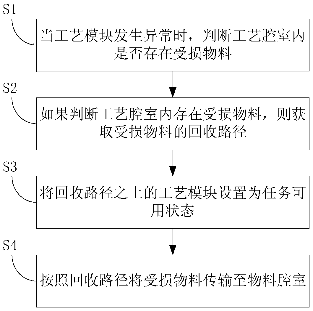
[0030] figure 1 is a flowchart of a semiconductor process control method according to an embodiment of the present invention. Such as figure 1 As shown, the semiconductor process control method includes the following steps:

[0031] S1, when an abnormality occurs in the process module, it is judged whether there is damag...


PUM


Abstract

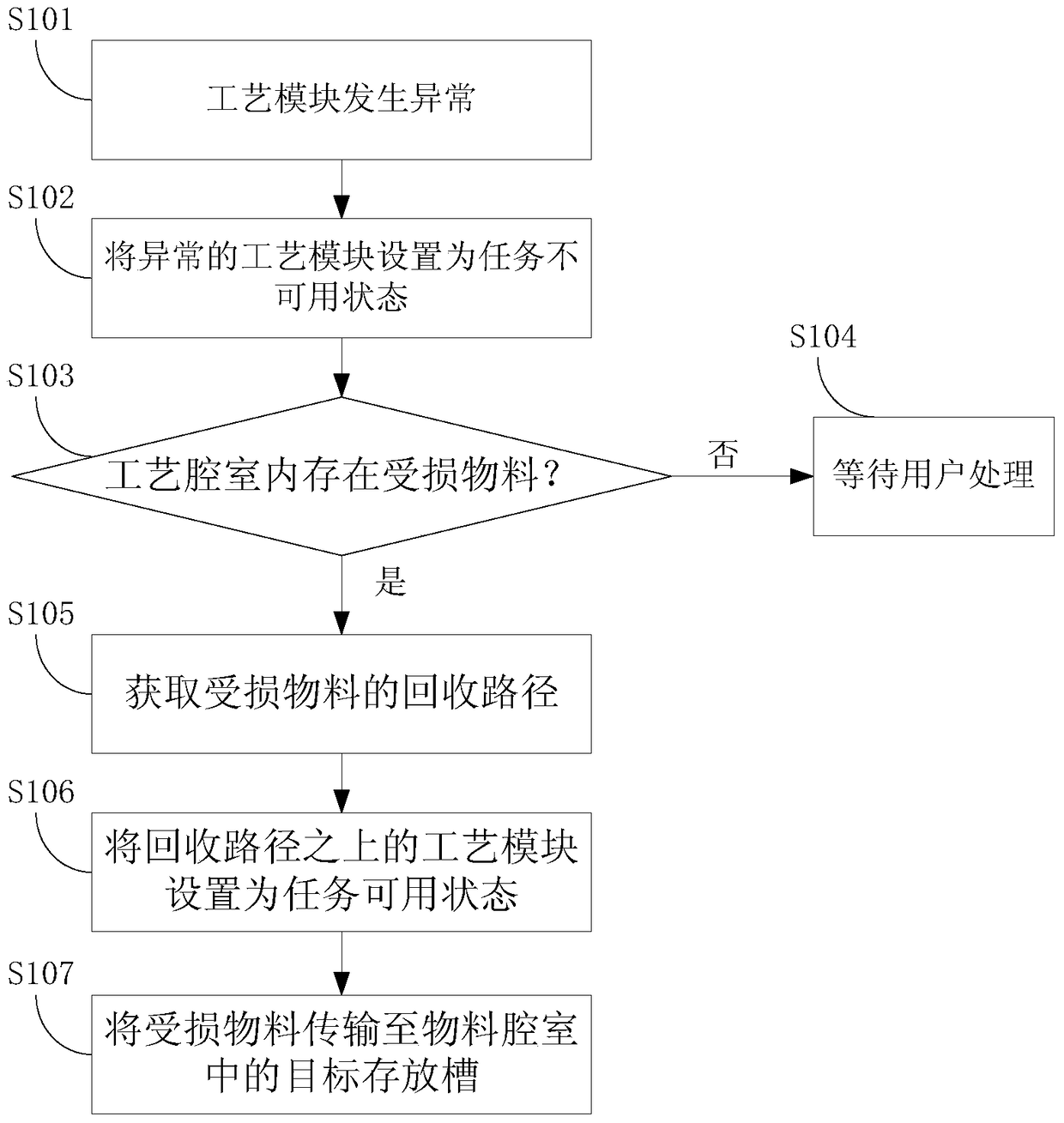
The invention discloses a semiconductor process control method and system, and the method comprises the steps: judging whether there is a damaged material in a technological cavity or not when an abnormality happens to a technological module; obtaining the recycle path of the damaged material if there is the damaged material in the technological cavity; setting the state of the technological module on the recycle path as a task usable state; and conveying the damaged object to a material cavity according to the recycle path. The method can automatically convey the damaged object to the material cavity when the abnormality happens to the technological module, prevents a worker from participating in the process, reduces the complexity of manual operation, saves the transmission time, and avoids the unstable transmission, caused by misoperation, of a machine platform.

Description

technical field [0001] The invention relates to the technical field of semiconductor technology, in particular to a semiconductor technology control method and a semiconductor technology control system. Background technique [0002] In the current semiconductor manufacturing process, the transfer of materials is very important. Usually, a transmission sequence is set at the program control end to control the reasonable and effective transmission of a large number of materials during the transmission process. However, due to various reasons, the process fails, so that the damaged materials cannot be automatically transmitted to the material chamber. [0003] Therefore, in the prior art, when damaged materials appear in the process chamber, the system will prompt and ask the operator whether to continue the transmission of the damaged materials. If the operator executes the command to continue the transmission, the damaged materials will be Transfer to the material chamber ac...

Claims


Application Information

Patent Timeline
Patent Type & Authority Patents(China)
IPC IPC(8): G05B19/418
CPCY02P90/02
Inventor 耿文毅
Owner BEIJING NAURA MICROELECTRONICS EQUIP CO LTD
Learn More