Interlayer dielectric layer forming method and semiconductor device forming method

A technology of interlayer dielectric layer and dielectric layer, which is applied in semiconductor/solid-state device manufacturing, electrical components, circuits, etc., can solve the problems that the quality of the interlayer dielectric layer cannot be guaranteed, the performance of the device is affected, and holes cannot be completely eliminated.

Inactive Publication Date: 2016-08-10
SEMICON MFG INT (SHANGHAI) CORP
View PDF4 Cites 2 Cited by
  • Summary
  • Abstract
  • Description
  • Claims
  • Application Information

AI Technical Summary

Problems solved by technology

[0004] However, in actual production, it is found that the quality of the interlayer dielectric layer is not ideal, which will affect the performance of the device
An important reason is that when

Method used


Image

  • Interlayer dielectric layer forming method and semiconductor device forming method
  • Interlayer dielectric layer forming method and semiconductor device forming method
  • Interlayer dielectric layer forming method and semiconductor device forming method

Examples


Embodiment Construction

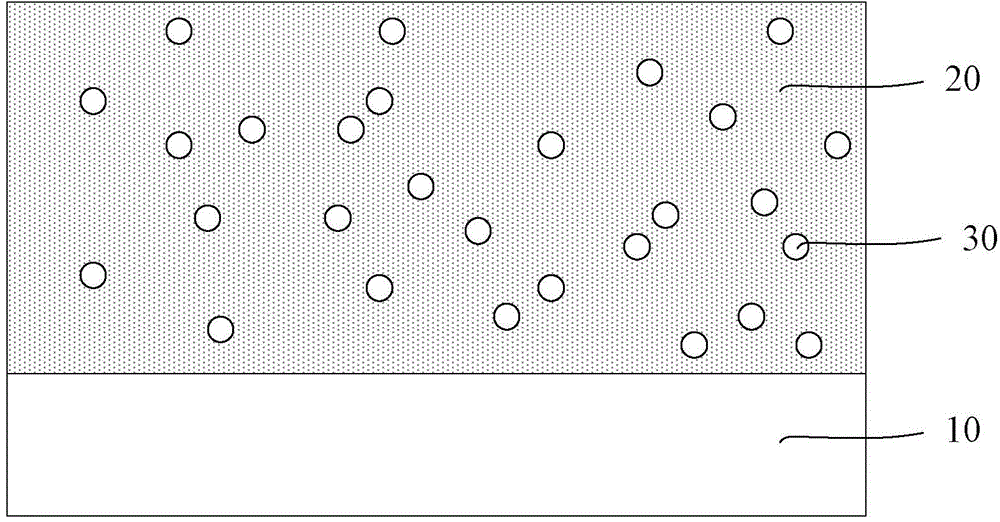
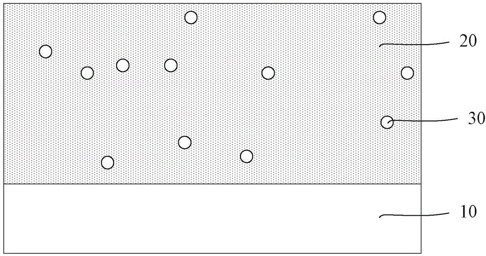
[0030] As mentioned in the background art, the quality of the current interlayer dielectric layer cannot meet the requirements. The inventors of the present application have found through long-term research that fluid chemical vapor deposition (FCVD) has been widely used in the formation of interlayer dielectric layers due to its advantages of strong hole filling. After the interlayer dielectric layer is formed by fluid chemical vapor deposition, an annealing process is usually required to remove holes that may appear in the interlayer dielectric layer during the formation process, improve the quality of the interlayer dielectric layer, and then perform an annealing process on the interlayer dielectric layer A subsequent etching process is performed. However, when the thickness of the interlayer dielectric layer is larger, more holes will be formed in the interlayer dielectric layer. Since some holes are far away from the surface of the interlayer dielectric layer, the common...


PUM


Abstract

In the method for forming an interlayer dielectric layer provided by the present invention, after the interlayer dielectric layer is formed by chemical vapor deposition, the interlayer dielectric layer is annealed for the first time, and then etched to form a contact hole. After the contact hole is formed, use the contact hole to increase the surface area of ​​the interlayer dielectric layer, and then perform the second annealing to completely eliminate the holes in the interlayer dielectric layer and improve the quality of the interlayer dielectric layer. When the thickness of the interlayer dielectric layer is relatively large, a better quality interlayer dielectric layer can also be obtained through this method. The present invention also provides a method for forming a semiconductor device. A device structure is previously formed in the substrate. After the second annealing, a wiring structure is formed through the contact hole to electrically connect the device structure. This method can simplify the process steps.

Description

technical field [0001] The invention relates to the field of semiconductors, in particular to a method for forming an interlayer dielectric layer and a method for forming a semiconductor device. Background technique [0002] With the development of high integration of semiconductor devices, the gate length of metal oxide semiconductor (MOS) devices is being scaled down to smaller sizes. Correspondingly, the manufacturing process of semiconductor devices is also being continuously improved to meet people's requirements device performance requirements. [0003] Depending on the type and function of the semiconductor device, the number of wiring layers of the manufactured semiconductor device will be different. A semiconductor device usually includes a device layer located on and within a semiconductor substrate, an interlayer dielectric layer (ILD) located above the device layer, and an active device and an inactive device located in the interlayer dielectric layer for connec...

Claims


Application Information

Patent Timeline
IPC IPC(8): H01L21/768
Inventor 胡建强邹陆军李绍彬
Owner SEMICON MFG INT (SHANGHAI) CORP
Why Eureka
Try Eureka