Substrate and mobile terminal

A mobile terminal and substrate technology, which is applied in the direction of printed circuits, printed circuits connected with non-printed electrical components, electrical components, etc., can solve the problem of affecting the connection effect of components and circuit patterns, affecting the working efficiency of substrates, and different processing depths, etc. Problems, to achieve the effect of improving product miniaturization and thinning, facilitating processing and thinning development, and improving the effect

Active Publication Date: 2016-08-10
HUAWEI DIGITAL POWER TECH CO LTD
View PDF5 Cites 2 Cited by
  • Summary
  • Abstract
  • Description
  • Claims
  • Application Information

AI Technical Summary

Problems solved by technology

[0003] However, in the prior art, when multiple devices are embedded in the same resin layer in the normal ECP processing flow, when multiple devices are applied to the embedded substrate, due to the different heights of the multiple devices, the buried structure in the prior art is difficult to guarantee The copper layer on the surface of the substrate has the same height from the pad of the device, which leads to different depths of the holes that need to be opened when the device is connected. During the production process, the processing depth of each hole is different, which greatly affects the substrate. The work efficiency during processing, and due to the difference in the embedding depth of the components, the size of the pads when the components are connected to the circuit pattern is different, and when the circuit pattern is formed, the connection effect between the components and the circuit pattern is affected.

Method used


Image

  • Substrate and mobile terminal
  • Substrate and mobile terminal
  • Substrate and mobile terminal

Examples


Embodiment Construction

[0022] In order to make the purpose, technical solutions and advantages of the present invention clearer, the present invention will be further described in detail below in conjunction with the accompanying drawings. Obviously, the described embodiments are only some of the embodiments of the present invention, rather than all of them. Based on the embodiments of the present invention, all other embodiments obtained by persons of ordinary skill in the art without making creative efforts belong to the protection scope of the present invention.

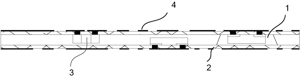
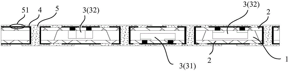
[0023] Such as figure 1 as shown, figure 1 A schematic structural view of the substrate provided by the embodiment of the present invention is shown.

[0024] In order to solve the above technical problems, a substrate is provided in this embodiment, on which a circuit pattern 4 and a plurality of components 3 are arranged, the substrate also includes: a resin layer 1 and a thin resin layer 2, a plurality of components 3 is embedded i...


PUM


Abstract

The invention relates to the electronic technical field, and discloses a substrate and a mobile terminal. The substrate possesses a circuit pattern and a plurality of components, and also comprises a resin layer and a thin resin layer, wherein the components are inlayed in the resin layer, and end faces of pins are flush with the surface of the resin layer; the thin resin layer is attached to the surface of the resin layer on which the pins of the components are exposed; the thin resin layer is provided with through holes corresponding to each pin; the circuit pattern is adhered to the surface of the thin resin layer deviating from the resin layer, and is in connection with bonding pads extending into each through hole and electrically connected to the pins. In the technical scheme device, device bonding pad surfaces in a same direction are all on a same plane, and thin resin is compressed, thereby meeting the requirement that the depths from device bonding pads to copper layers are the same, meanwhile reducing the sizes of bonding pads and the distance among bonding pads, facilitating processing, furthermore improving circuit pattern connection effects, and realizing reasonable module whole layout, and small and thin products.

Description

technical field [0001] The present invention relates to the field of electronic technology, in particular to a substrate and a mobile terminal. Background technique [0002] At present, the main purpose of adopting ECP technology in the industry is to improve product performance and higher integration; to develop in the direction of thinner and smaller product requirements. Embedded substrate: According to the substrate / PCB processing technology and component assembly characteristics, a new packaging technology that embeds components in the substrate / PCB; it improves product integration and reduces module dimensions; at the same time, it can improve product reliability. and electrothermal performance. [0003] However, in the prior art, when multiple devices are embedded in the same resin layer in the normal ECP processing flow, when multiple devices are applied to the embedded substrate, due to the different heights of the multiple devices, the buried structure in the prio...

Claims


Application Information

Patent Timeline
Patent Type & Authority Applications(China)
IPC IPC(8): H05K1/18
CPCH05K1/183H05K1/186H05K2201/10901H01L2224/04105H05K1/115H05K3/0035H05K3/282H05K3/421H05K2201/0191H05K2201/0376H05K2201/10477H05K2201/10545H05K2201/10674H05K2203/0156H05K2203/0207H05K2203/1316H05K2203/1469H05K2203/1476H05K2203/1572H05K3/0011H05K3/06H05K3/32H05K2201/10977H05K2203/1322
Inventor 鲍宽明
Owner HUAWEI DIGITAL POWER TECH CO LTD
Why Eureka
Try Eureka