Supercharge Your Innovation With Domain-Expert AI Agents!

Method for adding ink dot identification to MAP of prober

A MAP map and probe station technology, which is applied in the field of integrated circuit testing and manufacturing, can solve problems such as missing, and achieve the effect of improving equipment capacity and production efficiency

Active Publication Date: 2016-08-24
唐山捷准芯测信息科技有限公司
View PDF5 Cites 5 Cited by
  • Summary
  • Abstract
  • Description
  • Claims
  • Application Information

AI Technical Summary

Problems solved by technology

[0007] 2: The same format encoding, but the MAP lacking dot marks recognizes additional ink dots on the dot equipment

Method used


Image

  • Method for adding ink dot identification to MAP of prober
  • Method for adding ink dot identification to MAP of prober
  • Method for adding ink dot identification to MAP of prober

Examples


Embodiment Construction

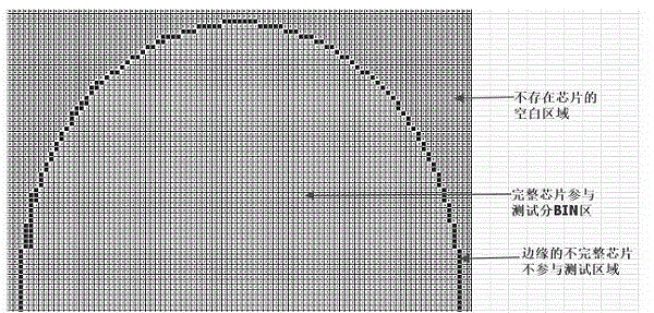
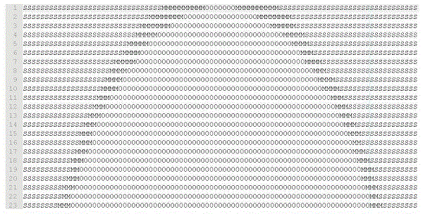
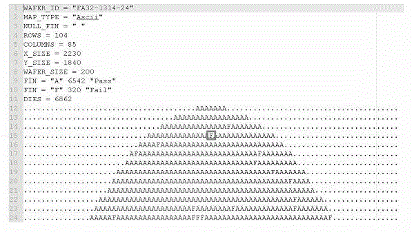
[0025] The present invention is used for the method for adding ink dots to the MAP map of the TSK UF series probe station, which comprises the following steps:

[0026] 1) Obtain the standard UF200 original image data that the wafer WAFER runs over the UF200 series probe station tester and call the MAP file.

[0027] 2) Open the MAP file in hexadecimal mode, extract the header file and the coordinates and identifier parameters of each chip according to the data format and length set by the UF200 probe station, and output it to the asicc-coded "UF200.txt "template.

[0028] 3) Use the text method to open the unified format of the MAP file that needs to be dotted, and convert it into the standard asicc coded "OTHER.txt" MAP file.

[0029] 4) Read the "OTHER.txt" file of asicc code that needs to be dotted, extract the row and column parameters of each chip, combine its position information in the "UF200.txt" template, restore it, and output it to "ink_MAP.txt" document.

[003...


PUM


Abstract

The invention provides a method for adding an ink dot identification to a MAP of a prober, and relates to the field of integrated circuit test and manufacture. The method comprises the following steps that 1) a UF200 original image data calling MAP file of an idle running standard of a wafer is obtained; 2) the MAP file is opened to extract a header file as well as coordinate and identifier parameters of each chip, and the header file and coordinate and identifier parameters are sent to a UF200.txt template of asicc coding; 3) the MAP file which needs dotting is opened in the unified format, and converted into an MAP file of OTHER.txt of standard asicc coding; 4) the OTHER.txt file, which needs dotting, of standard asicc coding is read to extract column and row parameters of each chip, the parameters are reduced by combining position information of the chip in the UF200.txt template, and output to an ink_MAP.txt file; and 5) the ink_MAP.txt file is opened to extract the header of the header file and coordinate and parameters of each chip to generate a UF200_ink_MAP. dat. The equipment capability and the production efficiency are improved.

Description

technical field [0001] The invention relates to the field of integrated circuit testing and manufacturing, in particular to a method for adding ink dot marks to a MAP map of a TSK UF series probe station in integrated circuit wafer manufacturing. Background technique [0002] Based on Moore's Law, the integrated circuit manufacturing process continues to improve, and the integration of chips is getting higher and higher. The diameter of the wafer has reached 300mm, and the characteristic linewidth of the chip has reached below 22nm. In the manufacturing process, the chip needs to be tested, reduced, and packaged. In these three links, the relevant information of the chip needs to be identified, shared and efficiently transmitted. Among them, the test system (ATE) and probe station (Prober) jointly complete the physical connection and test, and classify all chips through wafer testing: separate out failed and qualified chips for subsequent reduction and packaging. [0003] I...

Claims


Application Information

Patent Timeline
Patent Type & Authority Applications(China)
IPC IPC(8): H01L21/66G06F17/50
Inventor 欧阳睿王国兵肖金磊王生鹏朱万才邹欢
Owner 唐山捷准芯测信息科技有限公司
Features
  • R&D
  • Intellectual Property
  • Life Sciences
  • Materials
  • Tech Scout
  • Unparalleled Data Quality
  • Higher Quality Content
  • 60% Fewer Hallucinations
Learn More