Method for forming gate channel and corresponding semiconductor structure

A semiconductor and channel technology, applied in the direction of semiconductor devices, semiconductor/solid-state device manufacturing, semiconductor/solid-state device components, etc., can solve the problems of gate patterns that cannot be accurately aligned and alignment marks that cannot be measured, and achieve protection Effects that are not damaged

Active Publication Date: 2019-04-30
WUHAN XINXIN SEMICON MFG CO LTD
View PDF3 Cites 0 Cited by
  • Summary
  • Abstract
  • Description
  • Claims
  • Application Information

AI Technical Summary

Problems solved by technology

[0005] In view of the above-mentioned technical problems, the present invention aims to provide a method for forming a gate channel and a corresponding semiconductor structure to solve the problem in the prior art that the alignment mark cannot be measured due to the thick Kodiak film, which leads to subsequent channel etching. When the gate pattern cannot be precisely aligned

Method used


Image

  • Method for forming gate channel and corresponding semiconductor structure
  • Method for forming gate channel and corresponding semiconductor structure
  • Method for forming gate channel and corresponding semiconductor structure

Examples


Embodiment Construction

[0041] In the following description, numerous specific details are given in order to provide a more thorough understanding of the present invention. Of course, the present invention can also have other embodiments besides these detailed descriptions.

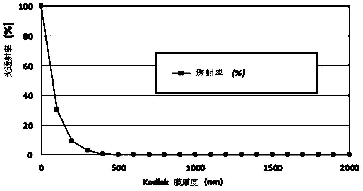
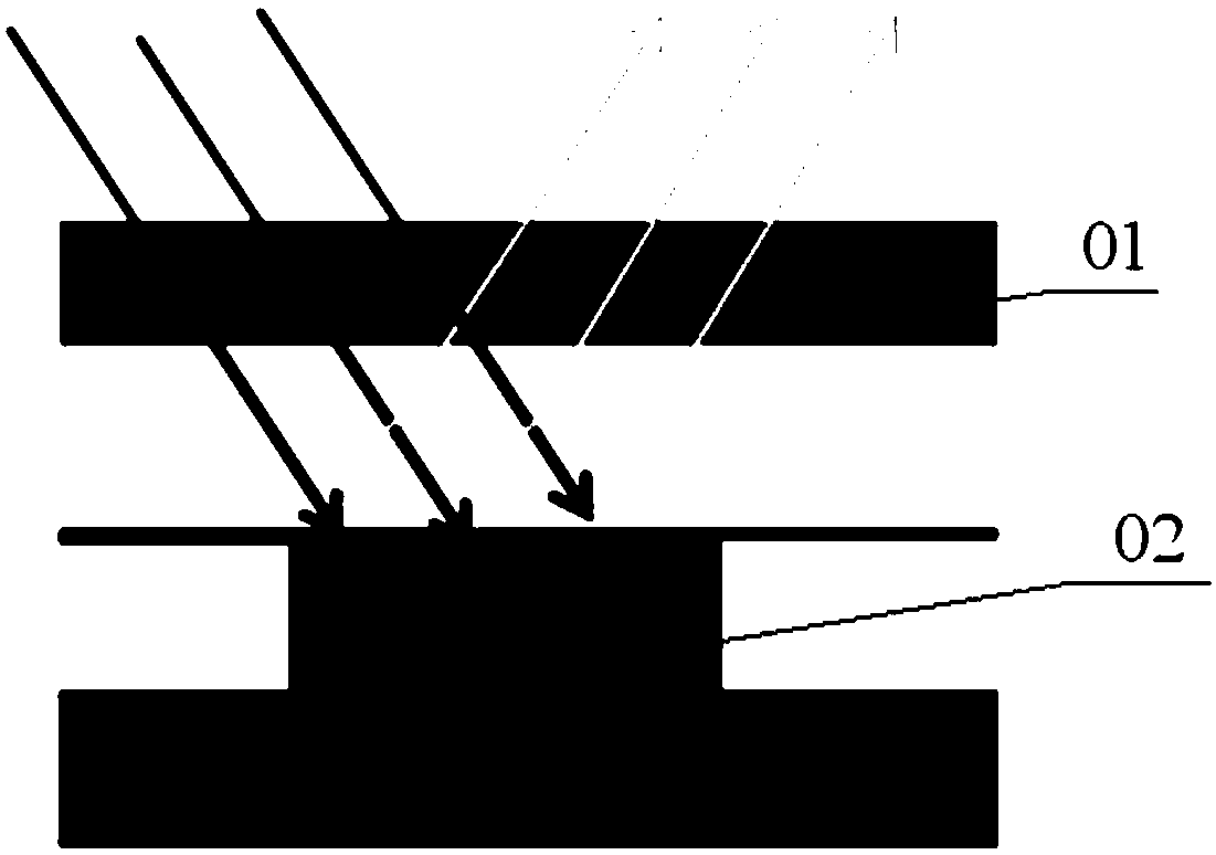
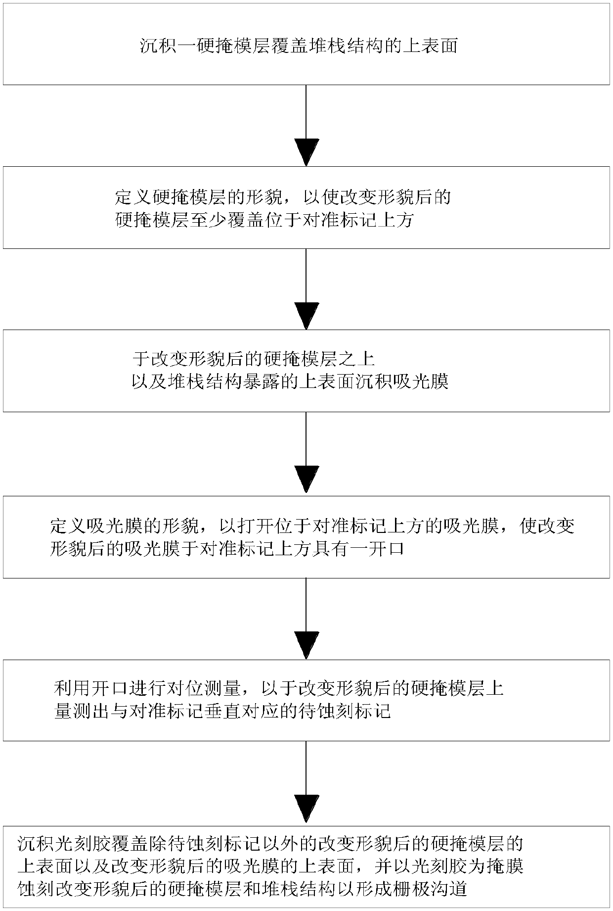
[0042] The method for forming a gate channel of the present invention is mainly applied to a stack structure in which an alignment mark (or called an overlay mark) is pre-embedded, such as image 3 As shown, it includes: depositing a hard mask layer first, and etching so that the hard mask layer covers at least the alignment marks; then depositing a light-absorbing film, and etching so that the light-absorbing film has an opening above the alignment marks; and then performing Alignment measurement, marking the gate channel corresponding to the mark to be etched on the hard mask layer; and then etching according to the mark to be etched to form the gate channel.

[0043] The steps of the method for forming a gate channel of the ...


PUM


Abstract

The present invention relates to the field of three-dimensional device fabrication, and in particular to a method for forming a gate channel and a corresponding semiconductor structure. By pre-burying an alignment mark in a stack structure, depositing a hard mask layer and etching it so that the hard mask layer is at least Covering is located above the alignment mark; then depositing a light-absorbing film and etching it so that the light-absorbing film has an opening above the alignment mark; then performing an alignment measurement, marking the gate channel corresponding to the alignment mark on the hard mask layer The to-be-etched mark; and then etch according to the to-be-etched mark to form a gate channel. In the present invention, by opening the light-absorbing film above the alignment mark, the incident light can be smoothly penetrated and reflected during the alignment measurement, so that the position of the alignment mark can be accurately measured, so as to ensure the accuracy of the grid when the channel is etched. Precise transfer of patterns.

Description

technical field [0001] The invention relates to the field of three-dimensional device fabrication, in particular to a method for forming a gate channel and a corresponding semiconductor structure. Background technique [0002] In the prior art, when producing a stacked memory to form a gate channel, it is usually necessary to deposit a thicker hard mask layer on top of the stacked structure (such as an alternately stacked 39-layer oxynitride layer) as an anti-reflection in the photolithography process. layer to ensure the morphology and critical dimensions of the gate channel after etching. [0003] However, when the thickness of the anti-reflection layer reaches a certain level (usually this thickness is much smaller than the thickness that can ensure the shape of the gate channel and the thickness of the key dimensions), it has a very high light absorption rate, and it cannot transmit light, which leads to the alignment used for etching. quasi-markers cannot be measured. ...

Claims


Application Information

Patent Timeline
Patent Type & Authority Patents(China)
IPC IPC(8): H01L21/28H01L21/033H01L21/66H01L23/544
Inventor 隋翔宇唐兆云高晶霍宗亮陆智勇许刚洪培真龚睿刘藩东何佳
Owner WUHAN XINXIN SEMICON MFG CO LTD
Why Eureka
Try Eureka