GaN Growth Method Based on Black Phosphorus and Magnetron Sputtering AlN

A magnetron sputtering and aluminum nitride technology, applied in the field of electronics, can solve the problems of limiting the selection range of substrates, large thermal expansion coefficient, affecting the quality of GaN materials, etc., and achieve the effect of reducing the number of common dislocation defects and improving the quality of materials

Active Publication Date: 2018-06-26
XIDIAN UNIV
View PDF5 Cites 0 Cited by
  • Summary
  • Abstract
  • Description
  • Claims
  • Application Information

AI Technical Summary

Problems solved by technology

However, the matching of silicon substrate and gallium nitride has the following problems: (1) has a large lattice mismatch; (2) has a large thermal expansion coefficient mismatch
However, the disadvantages of this method are: 1. The subsequent growth of GaN requires a high temperature above 1000°C, and graphene has poor thermal stability, and it will decompose at high temperature to generate carbon impurities, resulting in unintentional doping
2. The thickness of graphene is very thin, it is difficult to effectively alleviate the lattice mismatch between the substrate and gallium nitride, which greatly limits the selection range of substrates
However, the shortcomings of this method are: 1. Graphene is easy to decompose at high temperature to produce a large amount of C impurities, and the direct growth of GaN will make the impurities diffuse into the material and affect the material quality of GaN
2. The thickness of graphene is very thin, it is difficult to effectively alleviate the lattice mismatch between the substrate and gallium nitride, which greatly limits the selection range of substrates

Method used


Image

  • GaN Growth Method Based on Black Phosphorus and Magnetron Sputtering AlN
  • GaN Growth Method Based on Black Phosphorus and Magnetron Sputtering AlN

Examples


Embodiment 1

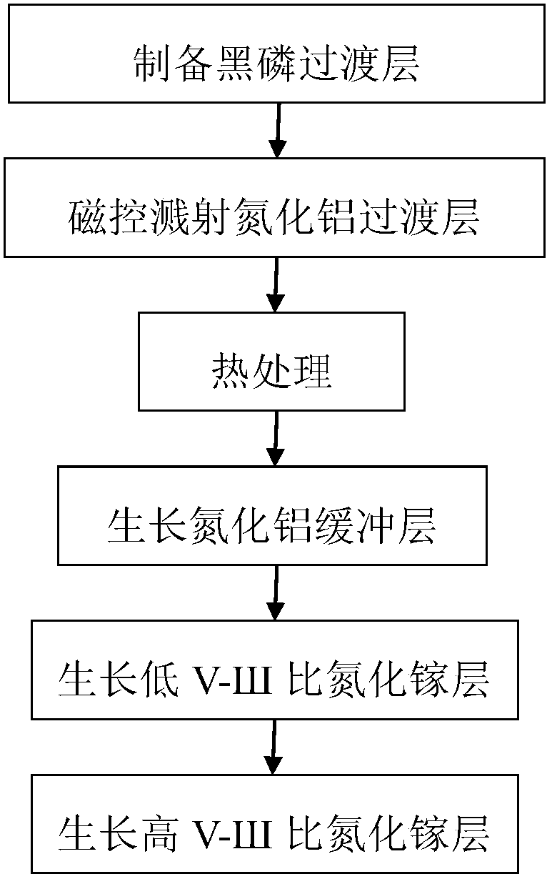
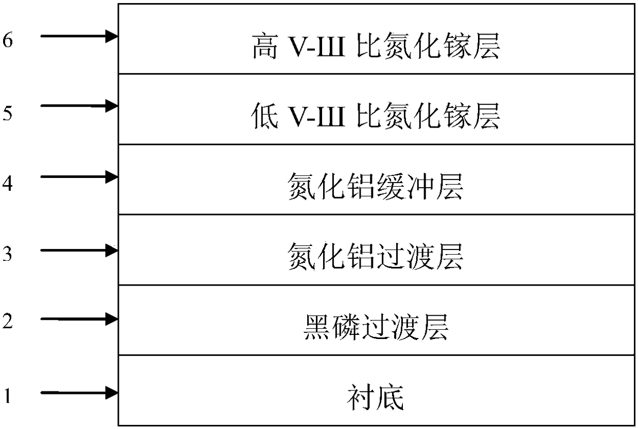
[0051] Embodiment 1: Ga-surface gallium nitride film based on black phosphorus and magnetron sputtering aluminum nitride.

[0052] Step 1. Prepare black phosphorus transition layer.

[0053] The silicon substrate was pretreated with acetone and deionized water and dried. Red phosphorus with a purity of 99.9% was put into a cube-shaped ultra-high pressure device, and the constant pressure in the cube-shaped ultra-high pressure device was set to 10 kbar. Keep the pressure of the cube-type ultra-high pressure device constant, heat the cube-type ultra-high pressure device to 1000°C, then cool down the temperature in the cube-type ultra-high pressure device by 100°C every hour until the temperature in the cube-type ultra-high pressure device reaches 600°C, close the cube Type ultra-high pressure device, wait for the temperature and pressure in the cube-type ultra-high pressure device to room temperature and normal pressure, take out the synthesized black phosphorus crystal, the pu...

Embodiment 2

[0065] Embodiment 2: N-face gallium nitride film based on black phosphorus and magnetron sputtering aluminum nitride.

[0066] Step A. Preparation of black phosphorus transition layer.

[0067] The sapphire substrates were pretreated with acetone and deionized water and dried. Red phosphorus with a purity of 99.9% was put into a cube-shaped ultra-high pressure device, and the constant pressure in the cube-shaped ultra-high pressure device was set to 10 kbar. Keep the pressure of the cube-type ultra-high pressure device constant, heat the cube-type ultra-high pressure device to 1000°C, then cool down the temperature in the cube-type ultra-high pressure device by 100°C every hour until the temperature in the cube-type ultra-high pressure device reaches 600°C, close the cube Type ultra-high pressure device, wait for the temperature and pressure in the cube-type ultra-high pressure device to room temperature and normal pressure, take out the synthesized black phosphorus crystal, ...


PUM

PropertyMeasurementUnit
thicknessaaaaaaaaaa
thicknessaaaaaaaaaa
thicknessaaaaaaaaaa

Abstract

The invention discloses a gallium nitride growth method based on black phosphorus and magnetron sputtering aluminum nitride. The method is mainly used for improving the quality of gallium nitride material. The growth step is as follows: (1) preparing a black phosphorous transition layer; (2) a magnetron sputtering aluminum nitride transition layer; (3) thermally treating; (4) growing an aluminum nitride buffer layer; (5) growing a low V-III ratio gallium nitride layer; (6) growing a high V-III ratio gallium nitride layer. The gallium nitride film disclosed by the invention has the advantages that the black phosphorus and magnetron sputtering aluminum nitride are combined, the material is excellent in quality, the applicable substrate range is large, and the gallium nitride film can be used for manufacturing high-performance gallium nitride-based device.

Description

technical field [0001] The invention belongs to the field of electronic technology, and further relates to a gallium nitride growth method based on black phosphorus and magnetron sputtering aluminum nitride in the field of microelectronic technology. The invention can be used for making gallium nitride thin films and devices thereof. Background technique [0002] The third-generation semiconductors represented by gallium nitride have the advantages of large band gap, high breakdown field strength, high thermal conductivity, corrosion resistance and radiation resistance, and are widely used in optoelectronic devices and electronic devices. Recent progress in the growth of GaN-based materials on silicon substrates and their device applications has attracted great attention. However, the following problems exist in the matching of silicon substrate and gallium nitride: (1) large lattice mismatch; (2) large thermal expansion coefficient mismatch. These will lead to high defect...

Claims


Application Information

Patent Timeline
Patent Type & Authority Patents(China)
IPC IPC(8): H01L21/02
CPCH01L21/0237H01L21/02458H01L21/02502H01L21/0254H01L21/0262H01L21/02631
Inventor 张进成朱家铎陈智斌庞凯吕佳骐许晟瑞林志宇宁静张金郝跃
Owner XIDIAN UNIV
Why Eureka
Try Eureka