Chip test method and device

A technology for chip testing and tested chips, which is applied in the field of chip testing methods and devices, can solve problems such as high cost of implementation, easy interference of excitation signals from the outside, and achieve the effects of cost saving and signal stability

Inactive Publication Date: 2016-09-07
SHENZHEN GOODIX TECH CO LTD
View PDF10 Cites 6 Cited by
  • Summary
  • Abstract
  • Description
  • Claims
  • Application Information

AI Technical Summary

Problems solved by technology

[0005] However, the existing test technology has the following defects: the pressing module is directly connected to the excitation signal, and the wire must be drawn from the corresponding excitation signal TX pin on

Method used


Image

  • Chip test method and device
  • Chip test method and device
  • Chip test method and device

Examples


Embodiment Construction

[0046] Hereinafter, the implementation of the application will be described in detail with the drawings and embodiments, so as to fully understand and implement the implementation process of how the application uses technical means to solve technical problems and achieve technical effects.

[0047] The following embodiments of the present invention are described by taking a test of a fingerprint recognition chip as an example. However, it should be noted that the solution of the embodiment of the present invention is not limited to the test of a fingerprint recognition chip, and can also be used for testing other chips.

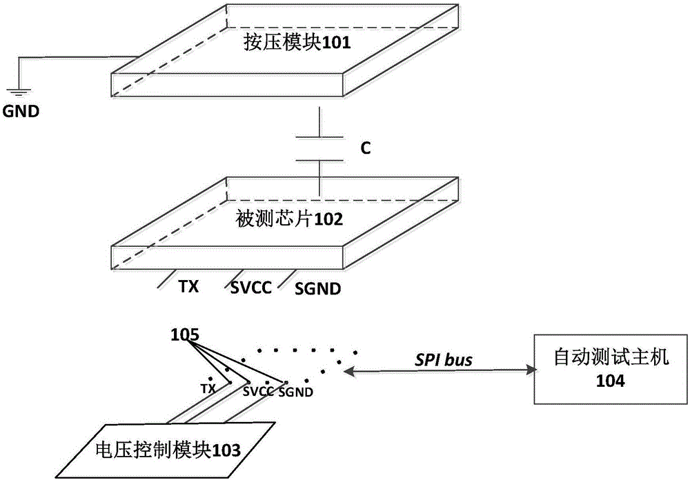
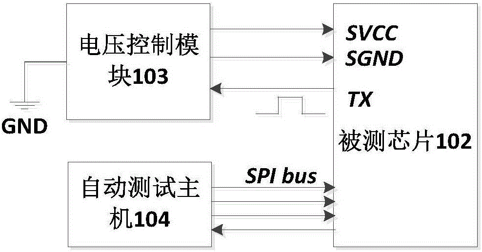
[0048] figure 1 Is a schematic diagram of the structure of a chip testing device according to an embodiment of the present invention; figure 1 As shown, in this embodiment, a chip test is taken as an example for description. Specifically, the test device includes: a pressing module 101, a voltage control module 103, and an automatic test host 104; the pressing mo...


PUM


Abstract

One embodiment of the invention provides a chip test device and a method. The device comprises a pressing module, a voltage control module and a test host computer; the pressing module is used for simulating gesture operation on tested chips and is electrically connected with constant signals; the test host computer is used for controlling the tested chips to output dynamically varied excitation signals; the voltage control muddle is used for dynamically regulating the test electrical signals of the tested chips to obtain equivalent fluctuation status of the excitation signals according to the dynamical variation of the excitation signals and rated electrical signals of the tested chips at normal operation; the test host computer is used for determining the test result according to the equivalent fluctuation status of the data excitation electrical signals obtained as test chips work under the equivalent fluctuation status of the excitation signals. According to the method and device, the pressing module is directly connected with constant electrical signals such as public reference ground connection without the need of excitation signal TX pin leading wires so that the cost of the system is saved. Besides, the pressing module is directly connected to the public reference ground which has relatively stable signals and will not be interfered by external signals.

Description

Technical field [0001] The embodiment of the present invention relates to chip testing technology, in particular to a chip testing method and device. Background technique [0002] Fingerprints are unique features of the human body, and their complexity is sufficient to provide sufficient features for identification. Therefore, fingerprint recognition technology is used in security, smart phones, time and attendance, access control, secure payment and other fields. The fingerprint recognition chip is the core device in fingerprint recognition technology to realize fingerprint image collection, feature extraction, feature comparison, etc. . The fingerprint identification chip needs to undergo strict quality testing before leaving the factory to ensure that the chip arriving at the client can be used normally. [0003] In the prior art, in order to facilitate post-processing and improvement of test efficiency, fingerprint identification chips are usually shipped in the form of subst...

Claims


Application Information

Patent Timeline
IPC IPC(8): G01R31/28
CPCG01R31/28
Inventor 杨炼覃伟和宋海宏管洲
Owner SHENZHEN GOODIX TECH CO LTD
Why Eureka
Try Eureka