Electrooptical lumped modulator
A modulator and electro-optical technology, applied in the field of integrated optoelectronics, can solve the problems of energy consumption, size, and insertion loss cannot be taken into account, and achieve the effect of reducing energy consumption, reducing size, and improving utilization efficiency
- Summary
- Abstract
- Description
- Claims
- Application Information
AI Technical Summary
Problems solved by technology
Method used
Image

Examples
Example Embodiment
[0030] In order to make the objectives, technical solutions, and advantages of the embodiments of the present invention clearer, the following will clearly describe the technical solutions in the embodiments of the present invention with reference to the accompanying drawings in the embodiments of the present invention. Obviously, the described embodiments are the present invention. Invented some embodiments, but not all embodiments. Based on the embodiments of the present invention, all other embodiments obtained by those of ordinary skill in the art without creative work shall fall within the protection scope of the present invention.
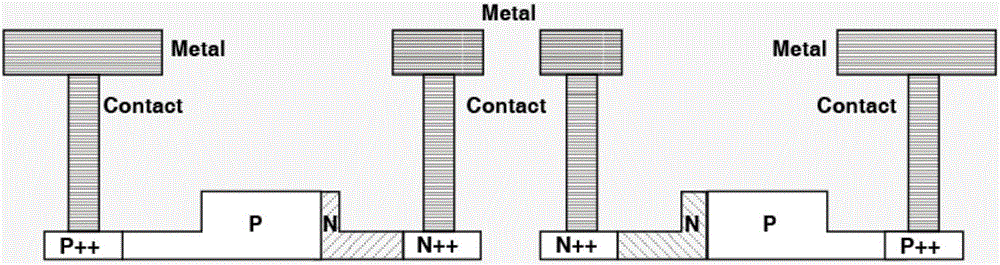
[0031] The existing lumped modulators mostly use such figure 1 The dual drive mode shown ( figure 1 The PN junction in is the simplest lateral junction, Metal stands for metal electrodes, Contact stands for metal vias), and its electro-optical bandwidth is only below 15GHz, which cannot meet the actual application requirements of modulation rates...
PUM
 Abstract
Description
Claims
Application Information
 - R&D Engineer
- R&D Manager
- IP Professional
- Industry Leading Data Capabilities
- Powerful AI technology
- Patent DNA Extraction
Browse by: Latest US Patents, China's latest patents, Technical Efficacy Thesaurus, Application Domain, Technology Topic.
© 2024 PatSnap. All rights reserved.Legal|Privacy policy|Modern Slavery Act Transparency Statement|Sitemap