Electroluminescent device and manufacturing method thereof

A technology of electroluminescent device and manufacturing method, which is applied in the direction of electro-solid device, semiconductor/solid-state device manufacturing, electrical components, etc., can solve problems such as energy loss of reflected light, and achieve the effect of shortening the propagation distance and reducing the degree of energy attenuation.

Active Publication Date: 2016-09-28
NANJING TECH CORP LTD
View PDF9 Cites 28 Cited by
  • Summary
  • Abstract
  • Description
  • Claims
  • Application Information

AI Technical Summary

Problems solved by technology

[0007] The invention provides an electroluminescent device and its manufacturing method, which solves the problem of loss of reflected light energy at the reflective electrode interface in the existing electroluminescent device

Method used


Image

  • Electroluminescent device and manufacturing method thereof
  • Electroluminescent device and manufacturing method thereof
  • Electroluminescent device and manufacturing method thereof

Examples


Embodiment 1

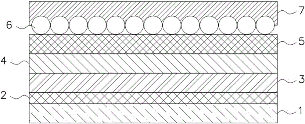
[0049] The present embodiment is an electroluminescence device, and its manufacturing method comprises:

[0050] (1) Cleaning of the ITO anode glass substrate: Use deionized water and ethanol to perform ultrasonic treatment on the ITO anode glass substrate in sequence. Cleaning treatment under oxygen plasma for 15 minutes;

[0051] (2) Fabrication of the hole injection and transport layer: in air, spin-coat PEDOT:PSS on the cleaned glass substrate at a speed of 2500rpm, and the spin-coating time is 50s; after the spin-coating is completed, anneal at 150°C in the air 30min, form the PEDOT:PSS layer (i.e. the hole injection layer), then on the PEDOT:PSS layer, spin-coat PVK chlorobenzene solution (concentration is 24mg / ml) with the rotating speed of 2000rpm, spin-coating time 60s; into the glove box, at N 2 Anneal at 150°C for 30 minutes in the atmosphere to form a PVK layer (ie, a hole transport layer);

[0052] (3) The making of quantum dot luminescent layer: quantum dot is...

Embodiment 2

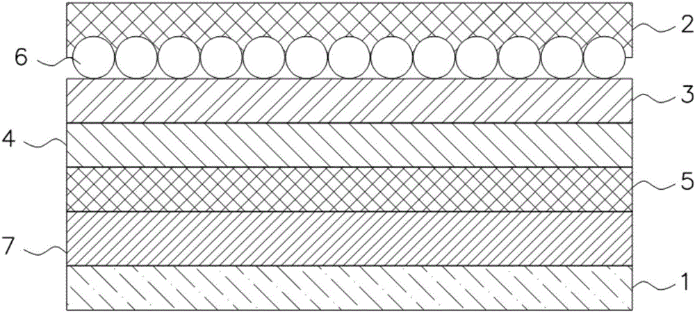
[0059] The present embodiment is an electroluminescence device, and its manufacturing method comprises:

[0060] (1) cleaning of ITO anode glass substrate: same as embodiment 1;

[0061] (2) The making of hole injection and transport layer: same as embodiment 1;

[0062] (3) The making of quantum dot luminescent layer: same as embodiment 1;

[0063] (4) The making of electron injection and transport layer: same as embodiment 1;

[0064] (5) The making of conductive particle layer: the ZnO nanocrystal of the band trioctylphosphine oxide ligand that particle diameter is 100nm is dispersed in toluene, obtains the ZnO toluene solution that solid content is 200mg / ml, on electron transport layer with The ZnO toluene solution was spin-coated at a speed of 2000rpm, and the spin-coating time was 60s, and a conductive particle layer was formed after drying;

[0065] After the conductive particle layer is made, use a step meter to measure the surface roughness of the conductive partic...

Embodiment 3

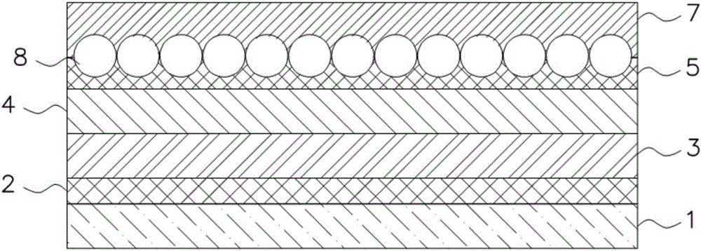
[0068] The present embodiment is an electroluminescence device, and its manufacturing method comprises:

[0069] (1) cleaning of ITO anode glass substrate: same as embodiment 1;

[0070] (2) The making of hole injection and transport layer: same as embodiment 1;

[0071] (3) The making of quantum dot luminescent layer: same as embodiment 1;

[0072] (4) The making of electron injection and transport layer: same as embodiment 1;

[0073] (5) The making of conductive particle layer: be that the ZnO nanocrystal of the band trioctylphosphine ligand of 200nm is dispersed in toluene with particle diameter, obtain the ZnO toluene solution that solid content is 100mg / ml, on electron transport layer with 2000rpm Spin-coat this ZnO toluene solution at a rotating speed of 60 seconds, and form a conductive particle layer after drying;

[0074] After the conductive particle layer is made, use a step meter to measure the surface roughness of the conductive particle layer, and the roughne...


PUM


Abstract

The invention discloses an electroluminescent device and a manufacturing method thereof. The electroluminescent device comprises a first electrode layer having transmissivity, a second electrode layer having reflectivity, a light-emitting layer arranged between the first electrode layer and the second electrode layer, and a second electrode layer contact layer adjacent to the second electrode layer; and the contact surface between the second electrode layer and the second electrode layer contact layer is a rough surface. According to the invention, the contact surface between the second electrode layer and the second electrode layer contact layer in the electroluminescent device is set to be a rough surface directly and lots of recessions and protrusions are distributed on the rough surface; and surface plasma waves are only be transmitted along the tangential directions of the contour lines of the recessions and the protrusions and thus the surface plasma wave propagation is limited and the surface plasma wave propagation distance is reduced substantially, so that the reflected light energy attenuation degree is reduced effectively.

Description

technical field [0001] The invention belongs to the technical field of semiconductors, and in particular relates to an electroluminescent device and a manufacturing method thereof. Background technique [0002] Light-emitting diodes (LEDs), as a new generation of lighting power sources, have the advantages of low energy consumption, low heat generation, and long life. As the core component of LED, luminescent material has a crucial influence on the performance of LED. [0003] Organic light-emitting diodes (OLEDs) and quantum dot light-emitting diodes (QLEDs) are currently the research hotspots of the new generation of LEDs. The multi-layer structure of QLED and OLED is similar, including sequentially stacked: substrate, anode, hole injection layer, hole transport layer, light-emitting layer, electron transport layer, electron injection layer, cathode; the main difference between the two is the light emission The light-emitting materials used in the different layers are di...

Claims


Application Information

Patent Timeline
Patent Type & Authority Applications(China)
IPC IPC(8): H01L51/50H01L51/52H01L51/56
CPCH10K50/00H10K50/805H10K71/00
Inventor 甄常刮陈超
Owner NANJING TECH CORP LTD
Why Eureka
Try Eureka