Chemical mechanical grinding equipment and method

A chemical-mechanical and grinding method technology, applied in grinding/polishing equipment, metal processing equipment, grinding machines, etc., can solve the problems of reduced production output, reduced thickness uniformity of ground silicon wafers, and reduced silicon wafer thickness uniformity, etc. To achieve the effect of reducing production costs, reducing waste production, and improving the pass rate

Active Publication Date: 2018-06-29
SEMICON MFG INT (SHANGHAI) CORP
View PDF5 Cites 0 Cited by
  • Summary
  • Abstract
  • Description
  • Claims
  • Application Information

AI Technical Summary

Problems solved by technology

[0004] Along with the grinding process, the surface of the grinding pad is also gradually worn and uneven during the grinding process. In this way, during the grinding process, for silicon wafers ground under the same pressure and rotation speed, the grinding rate will increase over time. changes, resulting in a decrease in the thickness uniformity of the polished silicon wafer
Since the existing chemical mechanical polishing process lacks an effective method for real-time monitoring of the thickness of the polished silicon wafer, the thickness of the silicon wafer and its changes during the grinding process cannot be obtained in real time, and it cannot be found in time: due to the wear and tear of the grinding pad The thickness uniformity of the polished silicon wafer is significantly reduced. If you continue to use the polishing pad for grinding, a large number of polished silicon wafers will be scrapped and the production output will be reduced.

Method used


Image

  • Chemical mechanical grinding equipment and method
  • Chemical mechanical grinding equipment and method
  • Chemical mechanical grinding equipment and method

Examples


Embodiment Construction

[0079] In order to make the above objects, features and advantages of the present invention more comprehensible, specific embodiments of the present invention will be described in detail below in conjunction with the accompanying drawings.

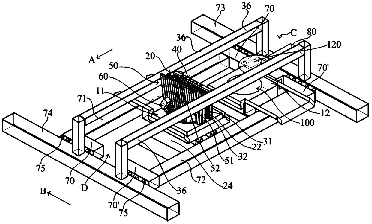
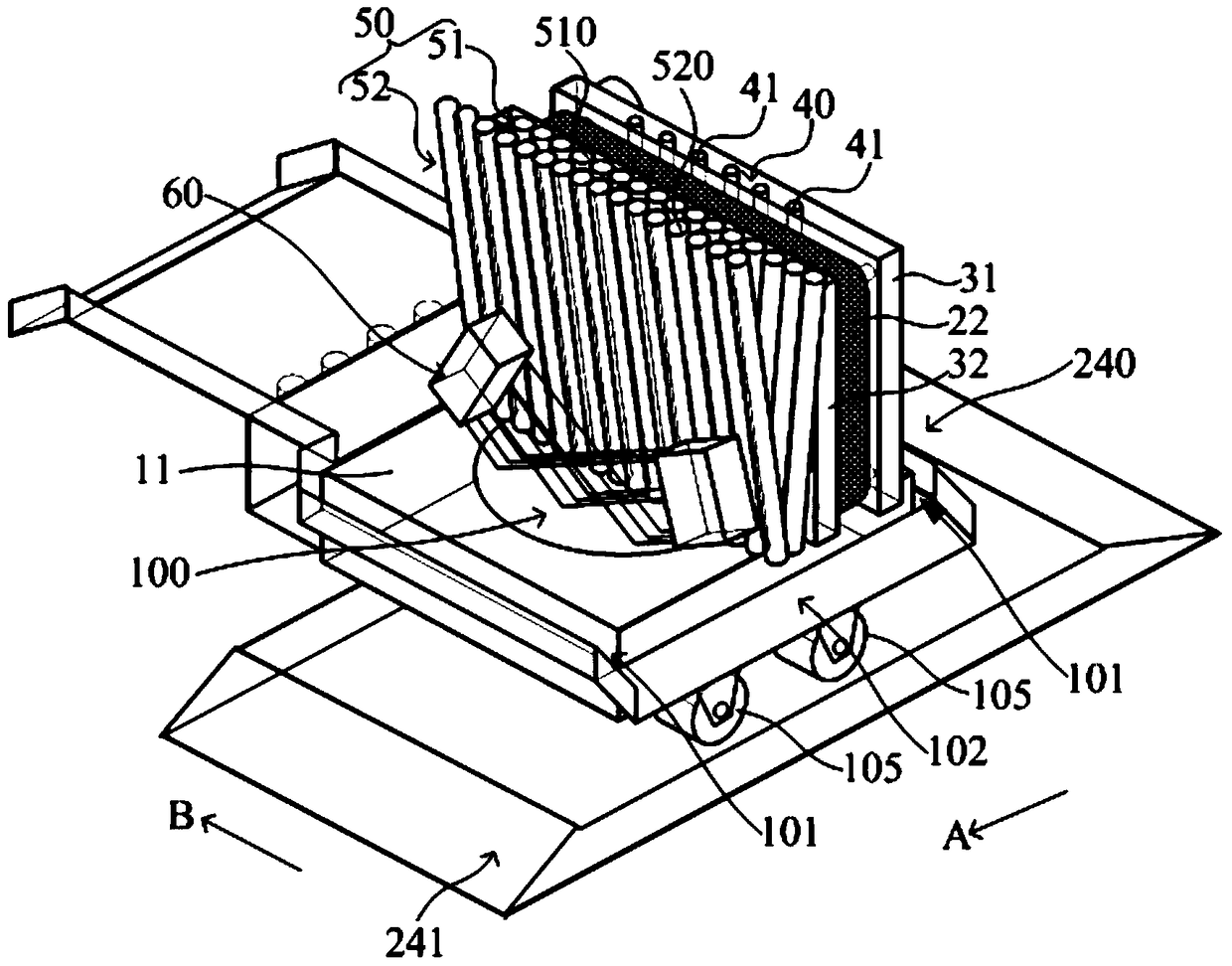
[0080] refer to Figure 2 ~ Figure 4 , the chemical mechanical grinding equipment of the present embodiment comprises:

[0081] The grinding area has a film inlet C and a film outlet D, and the direction from the film inlet C to the film outlet D is the first straight line direction A;

[0082] The first loading table 11 and the second loading table 12, each loading table upper surface is provided with a loading area 100, and in the grinding process, the wafer to be ground is placed on the loading area 100, and the two loading tables can be placed along the first Move in a straight line direction A;

[0083] The grinding mechanism 20 located in the grinding area includes: 4 pulleys 21, a grinding belt 22 sleeved on all the pulleys 21, an...


PUM


Abstract

A chemical mechanical polishing equipment and method, wherein the chemical mechanical polishing equipment includes: a slide table; a grinding mechanism, including a grinding piece capable of repeatedly moving along a second linear direction, and the first and second linear directions are perpendicular to each other; a polishing liquid injection mechanism , used to inject grinding liquid into the grinding piece; the grinding and cleaning mechanism is arranged opposite to the grinding mechanism along the first straight line; the film thickness measuring mechanism is used to measure the thickness of the cleaned piece to be ground. During the chemical mechanical grinding process, the moving piece to be ground is ground, cleaned and measured. Use this equipment to measure the thickness of the slices to be ground after grinding in real time, control the grinding amount of the slices to be ground during the grinding process, ensure that the thickness of the slices to be ground after grinding is the target thickness, improve the qualified rate of products, reduce the amount of waste slices, and reduce Cost of production.

Description

technical field [0001] The invention relates to the technical field of semiconductor manufacturing, in particular to a chemical mechanical polishing device and method. Background technique [0002] refer to figure 1 , figure 1 It is a schematic diagram of an existing chemical mechanical polishing equipment, which includes: a rotatable platform 1 ; a polishing pad 2 covering the platform 1 ; a rotatable polishing head 3 and a polishing liquid nozzle 4 . [0003] Taking a silicon wafer as an example, the method of chemical mechanical polishing is as follows: the silicon wafer 5 is turned upside down so that the surface to be polished contacts the grinding pad 2; then the grinding head 3 is pressed on the silicon wafer 5; then, the control platform 1 rotates and the rotation of the grinding head 3, while controlling the grinding fluid nozzle 4 to spray the grinding fluid 40 on the grinding pad 2, and applying downward pressure towards the silicon wafer 5 to the grinding head ...

Claims


Application Information

Patent Timeline
Patent Type & Authority Patents(China)
IPC IPC(8): B24B21/04B24B21/18B24B57/02B24B49/12
Inventor 伍强蒋运涛杨俊
Owner SEMICON MFG INT (SHANGHAI) CORP
Why Eureka
Try Eureka