Chip package structure and method of manufacturing the same
A chip packaging structure and chip technology, which is applied in the direction of electrical components, circuits, semiconductor devices, etc., can solve the problems of small application flexibility of light-emitting diode chip packaging structures, improve light conversion and output efficiency, prevent water vapor infiltration, and improve light output efficiency effect
- Summary
- Abstract
- Description
- Claims
- Application Information
AI Technical Summary
Problems solved by technology
Method used
Image

Examples
no. 1 example
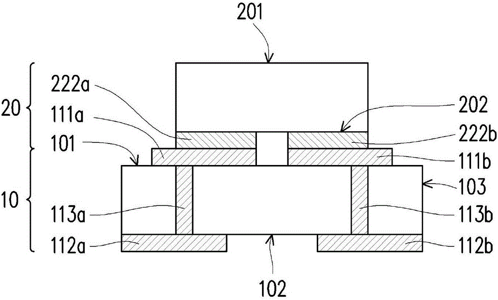
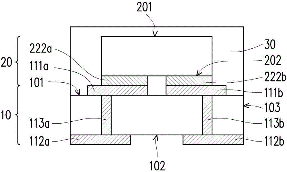
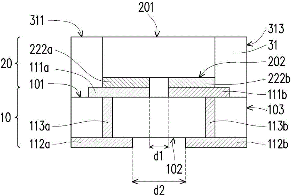
[0058] Figure 1A-1D It is a schematic diagram of a manufacturing method of a chip packaging structure according to the first embodiment of the present invention. Figure 1A-1D In the middle, the manufacturing method is illustrated with a cross-sectional illustration of a single chip package structure, so as to clearly describe the relevant details of each component. Such as Figure 1A As shown, a substrate 10 is provided, and a chip 20 is disposed on the carrying surface 101 of the substrate 10 . The chip 20, such as a light emitting diode chip, has a first surface 201 and a second surface 202 opposite to each other, and the second surface 202 is disposed on the carrying surface 101 of the substrate 10, and the first surface 201 is the light-emitting surface of the chip 20 .
[0059] In one embodiment, the chip 20 is a UV LED chip with a light emission wavelength between 315nm and 412nm. In another embodiment, the chip 20 is a blue light-emitting diode chip with a light emi...
no. 2 example
[0076] image 3 It is a schematic diagram of a chip packaging structure according to the second embodiment of the present invention. The difference between the second embodiment and the first embodiment is that Figure 1D A transparent layer 51 is further formed on the chip package structure shown. In the second embodiment, the transparent layer 51 is a planar transparent adhesive material. Such as image 3 As shown, the fluorescent layer 41 of the second embodiment is directly formed on the top surface 311 of the colloidal layer 31 and at least completely covers the first surface 201 of the chip 20, and the chip packaging structure further includes a light-transmitting layer 51 formed on the top of the colloidal layer 31 The fluorescent layer 41 is on and completely covers the surface 311 . The thickness of the transparent layer 51 is greater than that of the fluorescent layer 41 . Furthermore, in the second embodiment, the light-transmitting layer 51 has two side edges ...
no. 3 example
[0078] Figure 4 It is a schematic diagram of a chip package structure according to the third embodiment of the present invention. In the third embodiment also in such as Figure 1D A light-transmitting layer 52 is further formed on the chip package structure shown, but different from the second embodiment, the light-transmitting layer 52 of the third embodiment is a lens-type transparent adhesive material. Such as Figure 4 As shown, the transparent layer 52 of the third embodiment is formed on the top surface 311 of the colloidal layer 31 and completely covers the fluorescent layer 41 , and the upper surface 521 of the transparent layer 52 extends to the two side edges 313 of the colloidal layer 31 .
[0079] Both the planar light-transmitting layer 51 (the second embodiment) and the lens-type light-transmitting layer 52 (the third embodiment) can increase the water vapor transmission path and effectively prevent water vapor from infiltrating. The lens-type transparent la...
PUM
| Property | Measurement | Unit |
|---|---|---|
| Thickness | aaaaa | aaaaa |
| Particle size | aaaaa | aaaaa |
| Thickness | aaaaa | aaaaa |
Abstract
Description
Claims
Application Information