OSD interface switching scheme based on FPGA
An interface switching and solution technology, applied in the computer field, can solve the problems of many main chips and inconvenient circuit layout, and achieve the effect of reducing power consumption, saving the number of chips, and improving stability
- Summary
- Abstract
- Description
- Claims
- Application Information
AI Technical Summary
Problems solved by technology
Method used
Image

Examples
Embodiment Construction
[0016] The present invention will be further described below in conjunction with the accompanying drawings and specific embodiments.
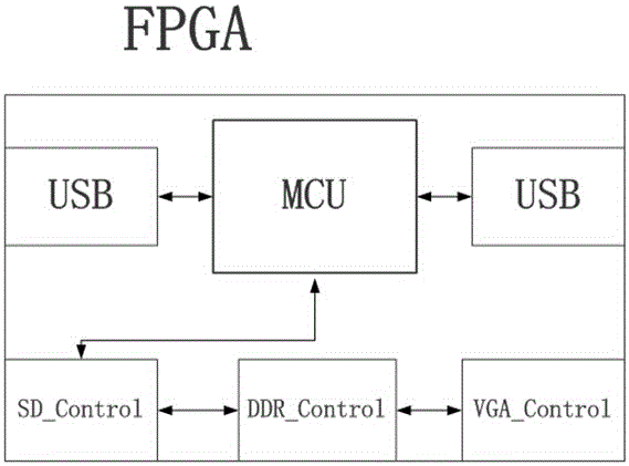
[0017] A kind of based on FPGA of the present invention realizes OSD interface switching scheme, its structure comprises:
[0018] Including PC, multi-unit server, ISE tool, keil tool;
[0019] A MC8051 IP core is embedded inside the FPGA as a control unit, and a hardware circuit is built inside the FPGA by a USB module, an SD module, a DDR module, and a VGA module;
[0020] Use the USB IP core and MCU to check the key value interception of the USB device, wait for the key value to call the OSD interface to be intercepted, and then send the command to read the picture to the SD card module through the MCU, and the SD card module will send the picture to the In the DDR control module, the DDR control module sends the stored picture information to the VGA display module, and sends it to the external display device through the VGA interface for d...
PUM
 Abstract
Description
Claims
Application Information
 - R&D
- Intellectual Property
- Life Sciences
- Materials
- Tech Scout
- Unparalleled Data Quality
- Higher Quality Content
- 60% Fewer Hallucinations
Browse by: Latest US Patents, China's latest patents, Technical Efficacy Thesaurus, Application Domain, Technology Topic, Popular Technical Reports.
© 2025 PatSnap. All rights reserved.Legal|Privacy policy|Modern Slavery Act Transparency Statement|Sitemap|About US| Contact US: help@patsnap.com