Method for manufacturing low-temperature polycrystalline silicon TFT array substrate and corresponding device

A low-temperature polysilicon and array substrate technology, which is used in semiconductor/solid-state device manufacturing, electrical components, and electrical solid-state devices, etc., can solve the problems of complex manufacturing process and increase the production cost of low-temperature polysilicon display equipment, so as to reduce production costs and reduce masking. The number of stencils, the effect of simplifying the process

Active Publication Date: 2016-10-12
BOE TECH GRP CO LTD
View PDF4 Cites 9 Cited by
  • Summary
  • Abstract
  • Description
  • Claims
  • Application Information

AI Technical Summary

Problems solved by technology

[0004] The embodiment of the present invention provides a method for manufacturing a low-temperature polysilicon TFT array su

Method used


Image

  • Method for manufacturing low-temperature polycrystalline silicon TFT array substrate and corresponding device
  • Method for manufacturing low-temperature polycrystalline silicon TFT array substrate and corresponding device
  • Method for manufacturing low-temperature polycrystalline silicon TFT array substrate and corresponding device

Examples


Embodiment Construction

[0037] The following will clearly and completely describe the technical solutions in the embodiments of the present invention with reference to the accompanying drawings in the embodiments of the present invention. Obviously, the described embodiments are only some, not all, embodiments of the present invention. Based on the embodiments of the present invention, all other embodiments obtained by persons of ordinary skill in the art without making creative efforts belong to the protection scope of the present invention.

[0038] The film thickness of each layer and the area shape and size in the drawings do not reflect the real proportion of the array substrate, but are only intended to schematically illustrate the content of the present invention.

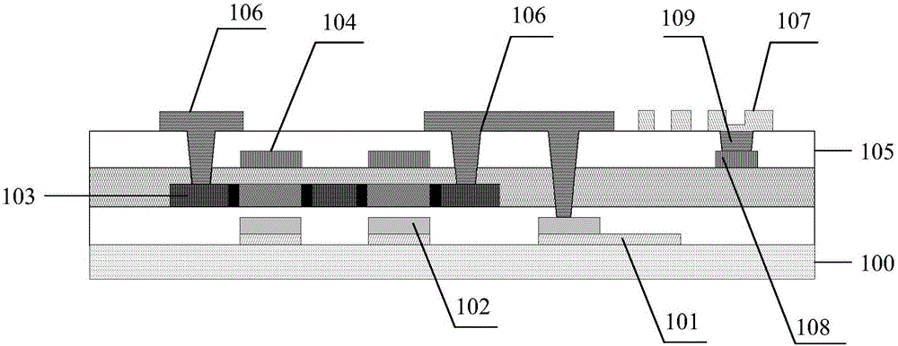
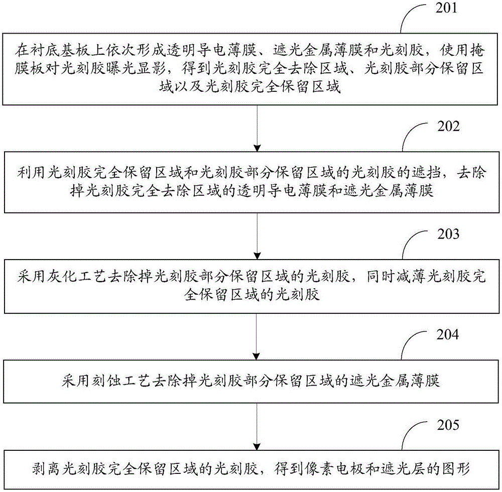
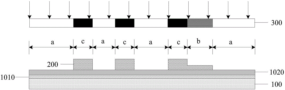
[0039] A method for manufacturing a low-temperature polysilicon TFT array substrate provided by an embodiment of the present invention includes the following steps: sequentially forming a pixel electrode, a light-shielding layer, a ...


PUM


Abstract

The invention relates to a method for manufacturing a low-temperature polycrystalline silicon TFT array substrate and a corresponding device. The method for manufacturing the low-temperature polycrystalline silicon TFT array substrate and the corresponding device are used for solving the problems that a current common LTPS process is complex in manufacturing process, 10-11 photolithography techniques need to be carried out generally, and consequently the production cost of low-temperature polycrystalline silicon display equipment is increased. The method comprises the steps that the graph of a pixel electrode, the graph of a shading layer, the graph of a low-temperature polycrystalline silicon active layer, the graph of a grid, the graph of an interlayer insulation layer, the graph of a source and drain and the graph of a common electrode are sequentially formed on an underlayer substrate; the graph of the pixel electrode and the graph of the shading layer are formed through one composition process. In the method for manufacturing the low-temperature polycrystalline silicon TFT array substrate, the graph of a pixel electrode layer and the graph of the shading layer can be formed through one composition process, the manufacturing process of the whole array substrate is achieved only through six composition processes, and compared with the mode that 10-11 photolithography techniques need to be carried out in the prior art, the number of mask plates used in the LTPS process is reduced, the manufacturing process is simplified, and the production cost is reduced.

Description

technical field [0001] The invention relates to the field of display panels, in particular to a method for manufacturing a low-temperature polysilicon TFT array substrate and a corresponding device. Background technique [0002] In pixel units of various display devices, a thin film transistor (Thin Film Transistor, TFT) that drives the display device by applying a driving voltage is widely used. Amorphous silicon (a-Si) materials with better stability and processability have been used in the active layer of TFTs, but amorphous silicon itself has its own defects, such as low on-state current and mobility due to too many defects. Low temperature and poor stability make it restricted in many fields. In order to make up for the defects of amorphous silicon and expand its application in related fields, low temperature polysilicon (LowTemperature Poly-Silicon, LTPS) technology came into being. Due to the high electron mobility of the liquid crystal display device using the LTPS ...

Claims


Application Information

Patent Timeline
IPC IPC(8): H01L27/12H01L21/77H01L27/15
CPCH01L21/77H01L27/12H01L27/1214H01L27/1259H01L27/127H01L27/1288H01L27/15H01L2021/775
Inventor 贺芳崔承镇
Owner BOE TECH GRP CO LTD
Why Eureka
Try Eureka