

Display device and preparation method thereof and electronic equipment
A technology for display devices and electronic equipment, which is applied to circuits, electrical components, and electrical solid devices, and can solve problems such as screen faults or layers, and overall uneven display effects
- Summary
- Abstract
- Description
- Claims
- Application Information
AI Technical Summary
Problems solved by technology
Method used
Image

Examples
Embodiment Construction
[0061] In order to make the technical solution of the present invention clearer, the present invention will be further described in detail below in conjunction with the accompanying drawings and specific embodiments.
[0062] First of all, it should be noted that the display device refers to a deformable and bendable display device made of soft materials.
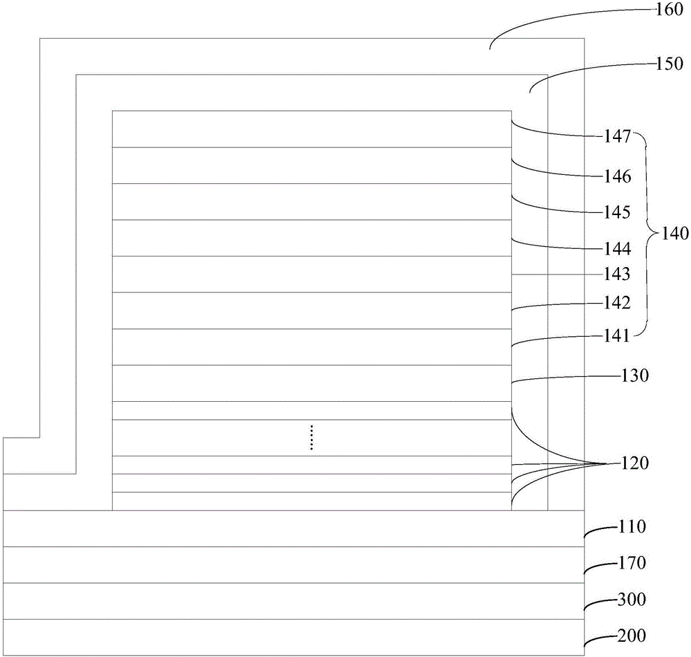
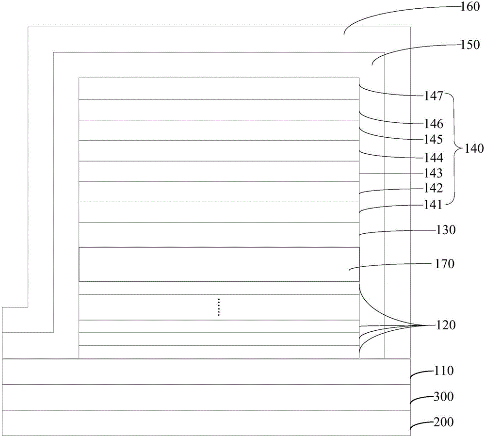
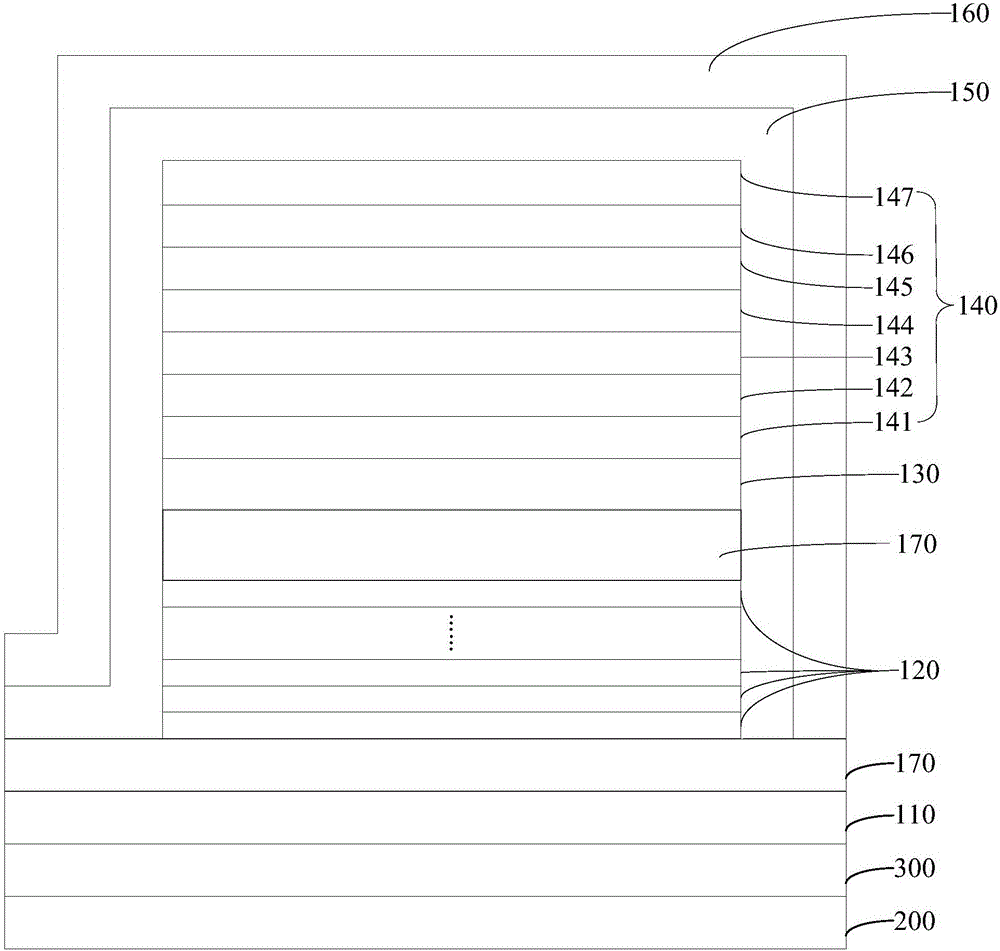
[0063] see Figure 1 to Figure 3 , as a specific embodiment of the display device of the present invention, it includes a substrate layer 110 , a TFT layer 120 , an anode layer 130 , an OLED layer 140 , a cathode layer 150 , an encapsulation layer 160 and a protective film 170 .
[0064] It should be noted that the substrate layer 110 refers to the BL (Buffer layer) layer prepared on the surface of the PI layer 300 after the PI (Polyimide) layer 300 is prepared on the surface of the substrate 200 by a spin-coating process during the preparation of the display device.
[0065]Further, the TFT layer 120 refers to a TFT (Thin...
PUM
 Abstract
Description
Claims
Application Information