Optical Proximity Correction Method

A technology of optical proximity correction and exposure graphics, which is applied in optics, originals for photomechanical processing, instruments, etc., can solve the problems that semiconductor devices cannot meet the design size requirements and the graphics are too small, so as to avoid the loss of yield rate, Avoid pinching or bridging effects

Active Publication Date: 2019-11-01
SEMICON MFG INT (SHANGHAI) CORP
View PDF5 Cites 1 Cited by
  • Summary
  • Abstract
  • Description
  • Claims
  • Application Information

AI Technical Summary

Problems solved by technology

[0006] However, in the existing technology, after optical proximity correction, the final pattern is often too small, and there will be a problem that the formed semiconductor device cannot meet the design size requirements.

Method used


Image

  • Optical Proximity Correction Method
  • Optical Proximity Correction Method
  • Optical Proximity Correction Method

Examples


Embodiment Construction

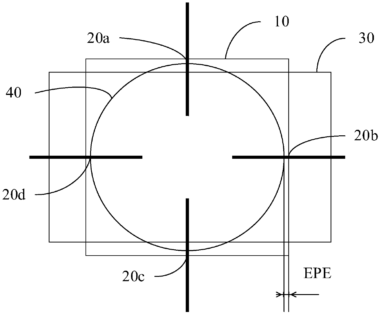
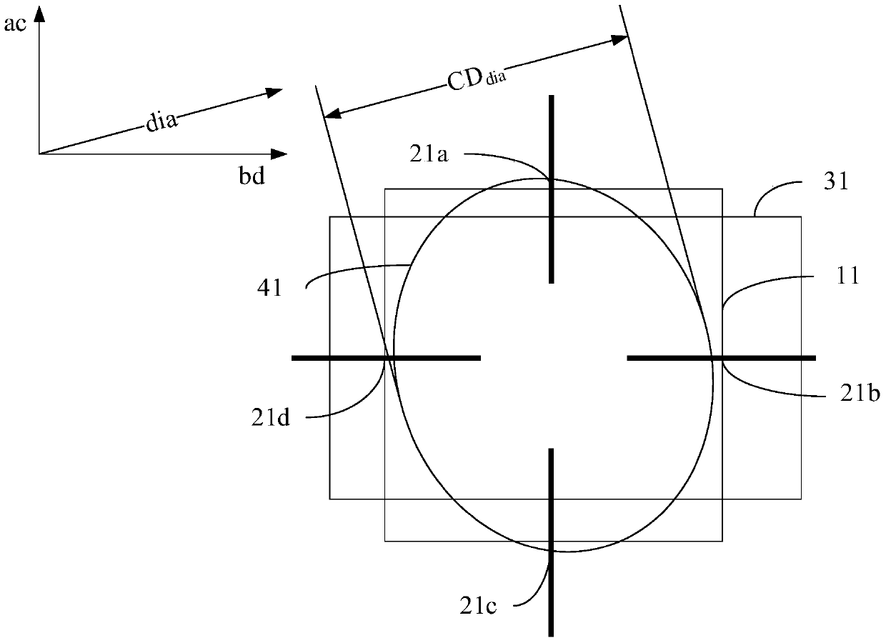
[0038] It can be known from the background art that the existing optical proximity correction technology has the problem that the formed semiconductor device cannot meet the design size requirement. Now, in combination with the existing technology, the optical proximity correction is performed on the pattern forming the contact hole to analyze the cause of the problem:

[0039]After the optical proximity correction is completed, if the edge position error in a certain direction reaches the standard, the size in this direction must also meet the design requirements. However, in the prior art, the method of taking a sampling point on each side of the target graphic, although after optical proximity correction, the size of the finally formed graphic in the direction of the sampling point must meet the design requirements. However, during the exposure process, the graphics may be distorted. When the graph is distorted, there may be an undersize problem in the direction where the ...


PUM


Abstract

The invention provides an optical proximity correction method. The correction method comprises the following steps: setting a plurality of sampling points on a target pattern, wherein the sampling points are on the corners or edges of the target pattern; setting a primary pattern; obtaining an exposed pattern corresponding to the primary pattern; obtaining the edge position error of the exposed pattern; judging whether the edge position error is greater than a preset threshold value, if the edge position error is less than or equal to the preset threshold value, obtaining the corrected pattern; if the edge position error is greater than the preset threshold value, adjusting the primary pattern; subjecting the adjusted primary pattern to previous steps (obtaining the exposed pattern and comparing) until the edge position error of the exposed pattern is less than or equal to the threshold value so as to finish the optical proximity correction to obtain the corrected pattern. The provided method has the advantages that the sampling points are increased to reduced the pattern distortion after optical proximity correction so as to solve the problem of insufficient feature size, which is caused by pattern distortion, of corrected pattern.

Description

technical field [0001] The invention relates to the field of semiconductor manufacturing, in particular to an optical proximity correction method. Background technique [0002] In the semiconductor manufacturing process, in order to transfer the circuit pattern of the integrated circuit (Integrated Circuit, IC) to the semiconductor chip, it is necessary to design the circuit pattern of the integrated circuit as a mask pattern, and then transfer the mask pattern from the surface of the mask to the semiconductor chip. chip. However, with the shrinking of the IC feature size (Critical Dimension, CD) and the impact of the resolution limit (Resolution Limit) of the exposure machine (Optical Exposure Tool, OET), when exposing the high-density mask pattern When the process is used for pattern transfer, it is easy to produce optical proximity effect (Optical Proximity Effect, OPE), which makes the mask pattern transfer defects. Aiming at the problem of the optical proximity effect...

Claims


Application Information

Patent Timeline
Patent Type & Authority Patents(China)
IPC IPC(8): G03F1/36
Inventor 杜杳隽
Owner SEMICON MFG INT (SHANGHAI) CORP
Why Eureka
Try Eureka