A kind of manufacturing method of silicon epitaxial wafer for coolmos
A manufacturing method and technology of silicon epitaxial wafers, which are applied in semiconductor/solid-state device manufacturing, electrical components, circuits, etc., can solve problems such as circuit pattern damage, slow polishing rate, low production efficiency, etc., to reduce impact and optimize surface quality. , the effect of eliminating the damage layer
- Summary
- Abstract
- Description
- Claims
- Application Information
AI Technical Summary
Problems solved by technology
Method used
Image

Examples
Embodiment 1
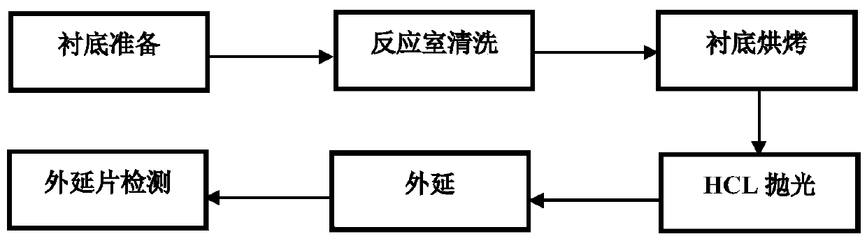
[0032] A method for manufacturing a silicon epitaxial wafer for COOLMOS of the present embodiment comprises the following steps:
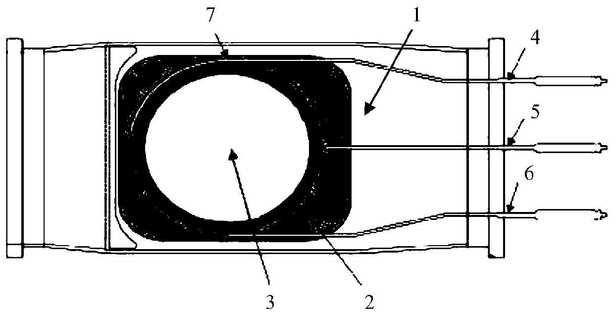
[0033] The equipment used in the present invention is the American ASM E2000 silicon epitaxial growth equipment, such as figure 2 As shown, the ASM E2000 silicon epitaxial growth equipment includes a pedestal 1, a pedestal ring 2 located on the pedestal 1, a central thermocouple 3 set in the pedestal ring 2, and also includes a front-end thermocouple 4, a rear-end thermocouple 5. Side-end thermocouple 6, side-end auxiliary thermocouple 7. The base is a high-purity graphite base and serves as an infrared heating body, and the purity of the main carrier gas H2 is above 99.9999%.
[0034] Cleaning of the reaction chamber: The quartz bell jar and the quartz parts used in the reaction chamber must be carefully cleaned before epitaxy, and the deposition residue on the inner wall of the quartz bell jar and the quartz parts must be completely removed.
...
Embodiment 2
[0043] The first four steps are described in the first embodiment.
[0044] Step 5: Gas etching is used to polish the surface of the silicon wafer. HCl gas with a flow rate of 1slm and H2 with a flow rate of 60slm are introduced for polishing. The polishing rate is 0.15μm / min, the polishing time is 3min, and the polishing thickness is 0.45μm. H in the fourth step 2 Bake at same temperature.
[0045] Step 6: After polishing, the temperature rises to 1190°C, and at the same time, the dopant source is expelled, and the expelled flow rate is determined according to the resistivity requirement of the epitaxial layer
[0046] Step 7: Epitaxial growth to control the thickness of the epitaxial layer: feed TCS, H2 and doping sources into the reaction chamber at the same time for epitaxial growth, feed TCS with a flow rate of 8g / min and H2 with a flow rate of 60slm, and the growth rate is 2.5μm / min . The flow rate of the doping source is determined according to the requirement of the...
Embodiment 3
[0048] The first four steps are described in the first embodiment.
[0049] The fifth step: gas corrosion to polish the surface of the silicon wafer, pass HCl gas with a flow rate of 0.8slm and H2 with a flow rate of 80slm for polishing, the polishing rate is 0.12μm / min, the polishing time is 2min, the polishing thickness is 0.24μm, and the polishing temperature and H in the fourth step 2 Bake at same temperature.
[0050] Step 6: After polishing, the temperature rises to 1170°C, and at the same time, the dopant source is expelled, and the expelled flow rate is determined according to the resistivity requirement of the epitaxial layer
[0051] Step 7: Epitaxial growth to control the thickness of the epitaxial layer: feed TCS, H2 and dopant sources into the reaction chamber at the same time for epitaxial growth, feed TCS at a flow rate of 6g / min and H2 at a flow rate of 80slm, and the growth rate is 2μm / min. The flow rate of the doping source is determined according to the re...
PUM
 Abstract
Description
Claims
Application Information
 - R&D Engineer
- R&D Manager
- IP Professional
- Industry Leading Data Capabilities
- Powerful AI technology
- Patent DNA Extraction
Browse by: Latest US Patents, China's latest patents, Technical Efficacy Thesaurus, Application Domain, Technology Topic.
© 2024 PatSnap. All rights reserved.Legal|Privacy policy|Modern Slavery Act Transparency Statement|Sitemap