Optical structure and display substrate
A technology of optical structure and structural unit, applied in optics, nonlinear optics, instruments, etc., can solve problems such as unsatisfactory viewing angle and light output rate, lower cathode emissivity, low light output rate, etc.
- Summary
- Abstract
- Description
- Claims
- Application Information
AI Technical Summary
Problems solved by technology
Method used
Image

Examples
Embodiment 1
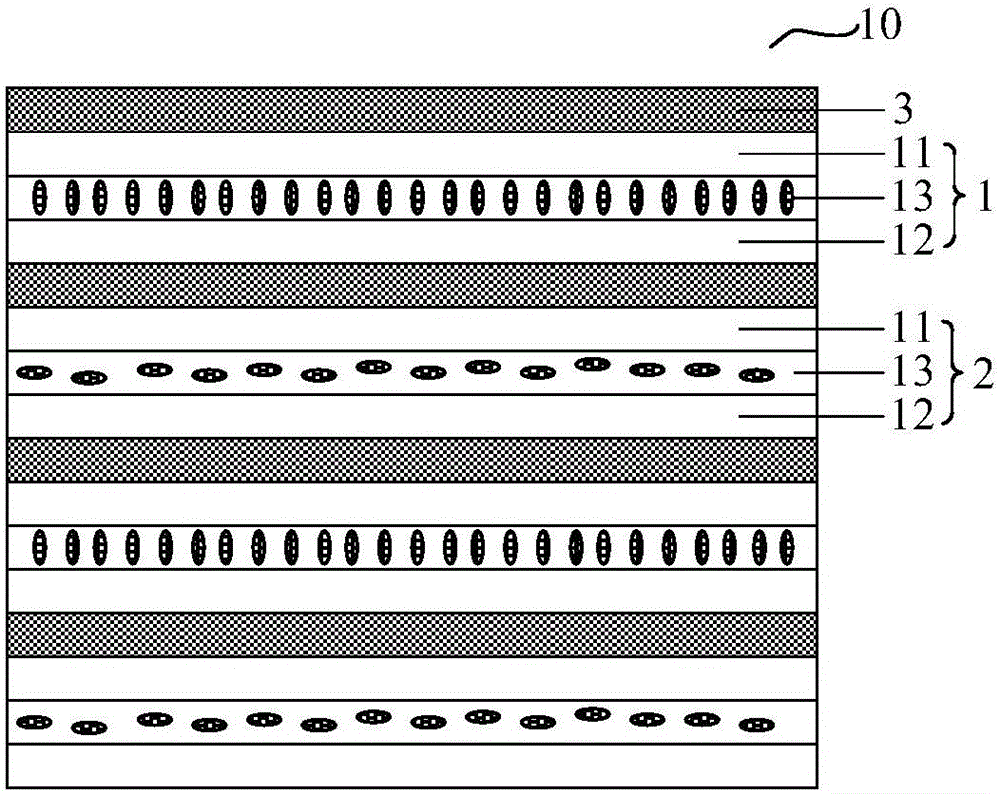
[0024] Please refer to figure 1 , this embodiment provides an optical structure 10, including first structural units 1 and second structural units 2 arranged alternately, the refractive index of the first structural unit 1 and the refractive index of the second structural unit 2 are adjustable, so as to The refractive indices of the first structural unit 1 and the second structural unit 2 are made different.
[0025] From figure 1 It can be seen from the figure that the first structural unit 1 and the second structural unit 2 are stacked, that is to say, when the number of the second structural unit 2 and the first structural unit 1 are multiple, the " The structure of the second structural unit 2—the first structural unit 1—the second structural unit 2—the first structural unit 1…”; when the number of the second structural unit 2 and the first structural unit 1 is one, the first structure Unit 1 is located above the second structural unit 2 .
[0026] Wherein, both the fir...
Embodiment 2
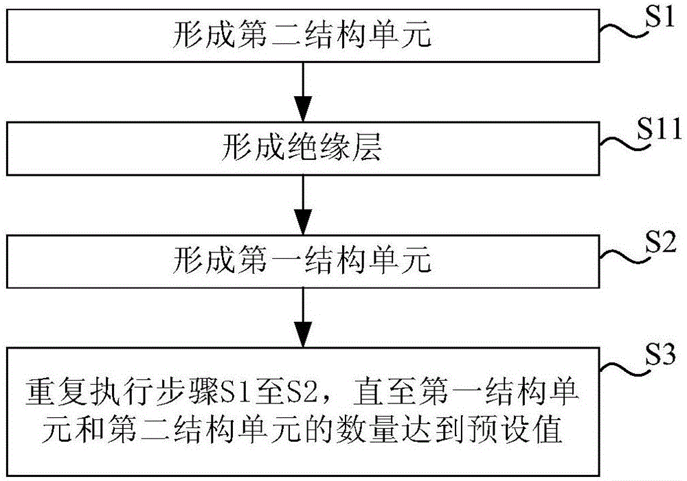
[0050] Please refer to figure 2 , this embodiment provides a method for preparing an optical structure, including:
[0051] The first structural unit 1 and the second structural unit 2 are alternately formed; the refractive index of the first structural unit 1 and the refractive index of the second structural unit 2 are adjustable, so that the first structural unit 1 and the second structural unit 2 The refractive index is different.
[0052] Wherein, alternately forming the first structural unit 1 and the second structural unit 2 specifically includes:
[0053] S1, forming a second structural unit 1;
[0054] S2, forming the first structural unit 2.
[0055] Wherein, between step S1 and step S2, it also includes:
[0056] S11, forming an insulating layer 3 .
[0057] Wherein, if the number of the first structural unit 1 and the second structural unit 2 is greater than 1, the preparation method further includes:
[0058] S3. Repeat steps S1 to S2 until the number of the...
Embodiment 3
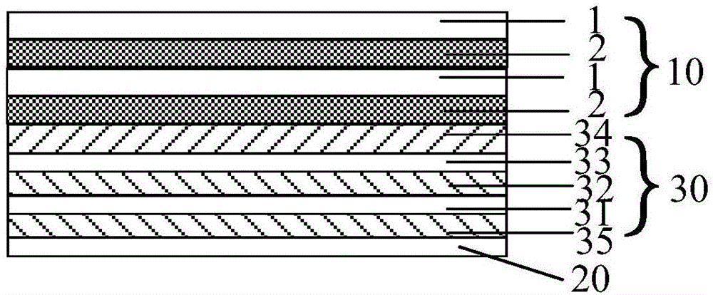
[0062] Please refer to image 3 and Figure 4 , this embodiment provides a display substrate, including a base substrate 20, a light-emitting device 30 and the optical structure 10 of Embodiment 1, the light-emitting device 30 is located on the base substrate 20, and the optical structure 10 is located on the light-emitting side of the light-emitting device 30, Wherein, the light emitted from the light emitting side of the light emitting device 30 enters the optical structure 10 through the second structural unit 2 , and the refractive index of the second structural unit 2 is greater than that of the first structural unit 1 .
[0063] Wherein, the light-emitting device 30 includes conventional structures such as an array layer 35, an anode 31, an organic layer 32, a cathode 33, and an encapsulation layer 34 arranged in sequence. In this embodiment, the cathode 33 is a transparent electrode, and the anode 31 is a non-transparent electrode. It can be understood that the light e...
PUM
| Property | Measurement | Unit |
|---|---|---|
| Thickness | aaaaa | aaaaa |
| Thickness | aaaaa | aaaaa |
Abstract
Description
Claims
Application Information