Energy-saving jump-image-free integral imaging and displaying device based on grating waveguide

An integrated imaging and grating waveguide technology, applied in optics, optical components, instruments, etc., can solve the problems of inability to take into account imaging quality and processing technology, low utilization of light energy, etc., to improve the utilization of light and reduce light energy. The effect of consumption and quality improvement

Active Publication Date: 2016-11-16
北京敏光科技有限公司
View PDF7 Cites 13 Cited by
  • Summary
  • Abstract
  • Description
  • Claims
  • Application Information

AI Technical Summary

Problems solved by technology

[0005] The purpose of the present invention is to overcome the above-mentioned defects in the prior art, and propose an energy-saving non-jump image integrated imaging display device based on a grating waveguide, which i

Method used


Image

  • Energy-saving jump-image-free integral imaging and displaying device based on grating waveguide
  • Energy-saving jump-image-free integral imaging and displaying device based on grating waveguide
  • Energy-saving jump-image-free integral imaging and displaying device based on grating waveguide

Examples


Embodiment Construction

[0020] The present invention will be further described below in conjunction with the accompanying drawings and embodiments.

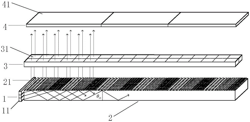
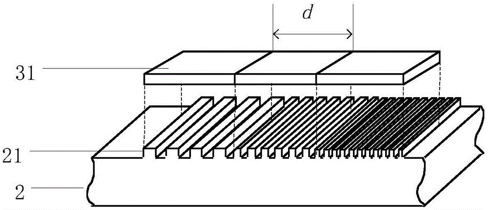
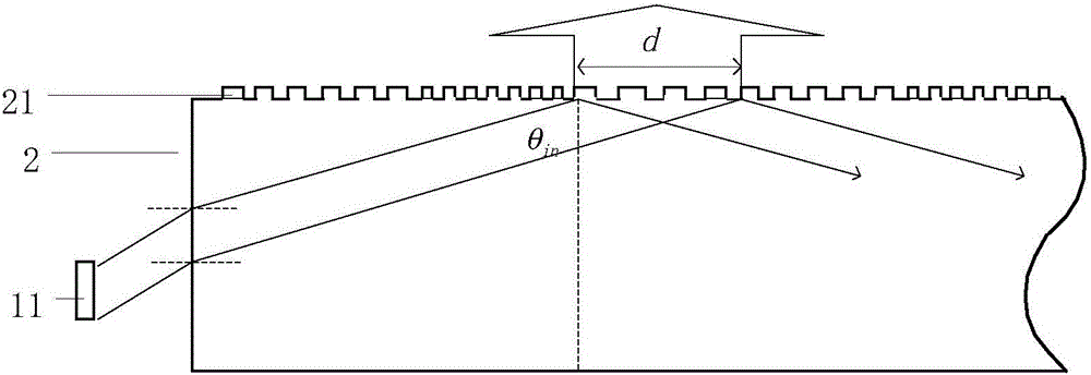
[0021] refer to figure 1 , a jump-free image integrated imaging display device based on grating waveguide, including LED light source, waveguide medium, display panel and microlens array, microlens array, display panel and waveguide medium are arranged in parallel in sequence, and the vertical center of the three The axes are coincident and the horizontal central axes are parallel. The horizontal cross-sections of the waveguide medium, display panel and microlens array used in this embodiment are rectangles with equal length and width, and the LED light source is located on the left side of the waveguide medium.

[0022] The parameters of the microlens array are equal to the parameters of the microlens array used by the integrated imaging system to record the three-dimensional light field information in object space. One image unit corresponds.

[002...


PUM


Abstract

The invention provides an energy-saving jump-image-free integral imaging and displaying device based on grating waveguide, which is used to solve the technical problem that existing integral imaging and displaying devices have low light energy utilization rate and cannot balance the imaging quality and the processing technology. The energy-saving jump-image-free integral imaging and displaying device based on grating waveguide comprises an LED light source, a waveguide medium, a display panel and a microlens array. The LED light source is an array light source formed by red, green and blue three-primary-color LED lights. The display panel is a liquid crystal panel without a color filter. A grating which consists of a plurality of periodically-arranged grating elements is disposed on the surface, adjacent to the display panel, of the waveguide medium. Each grating element comprises three grating regions corresponding to the periods of red, green and blue three-primary-color light, from large to small. The microlens array, the display panel and the waveguide medium are sequentially arranged in parallel. The LED light source is located at the side of the waveguide medium. Light emitted from the LED light source is irradiated onto the corresponding grating region, and light emitted from the region can be vertically irradiated only onto a light channel, corresponding to the region, on the display panel.

Description

technical field [0001] The invention belongs to the technical field of integrated imaging three-dimensional display, in particular to integrated imaging three-dimensional display, in particular to an energy-saving and jump-free image integrated imaging display device based on a grating waveguide, which is used to reproduce three-dimensional information in object space. Background technique [0002] The integrated imaging 3D display technology includes two stages of recording and display. The recording stage is to use the microlens array to record the three-dimensional object space information and obtain the microimage array; the display stage is to use the microlens array with the same parameters as the microlens array used in the recording stage to The light emitted by the micro-image array is converged and restored to reconstruct the three-dimensional light field information in the object space. The concept of integrated imaging three-dimensional display technology was fir...

Claims


Application Information

Patent Timeline
IPC IPC(8): G02B27/22
CPCG02B30/27
Inventor 王晓蕊郭丹凤张建磊穆江浩袁影
Owner 北京敏光科技有限公司
Why Eureka
Try Eureka