Method for realizing degradation of stacked IC defective products through cutting break line of package body

A package and bad technology, applied in semiconductor/solid-state device manufacturing, semiconductor/solid-state device testing/measurement, electrical components, etc., can solve problems such as increasing revenue, scrapping the entire IC, and malfunctioning, to increase operating income , accurate cutting, and the effect of reducing waste

Active Publication Date: 2016-11-23
TEKISM
View PDF4 Cites 2 Cited by
  • Summary
  • Abstract
  • Description
  • Claims
  • Application Information

AI Technical Summary

Problems solved by technology

[0003] In order to solve the problem in the prior art that one of the multiple dies is damaged or malfunctions causing the entire IC to be scrapped, the present invention discloses that the cutting position of the die is determined accurately through calculation, so that the cutt

Method used


Image

  • Method for realizing degradation of stacked IC defective products through cutting break line of package body
  • Method for realizing degradation of stacked IC defective products through cutting break line of package body
  • Method for realizing degradation of stacked IC defective products through cutting break line of package body

Examples


Embodiment Construction

[0024] The present invention will be further described below in conjunction with the accompanying drawings. It should be understood that the specific embodiments described here are only used to explain the present invention, and are not intended to limit the present invention.

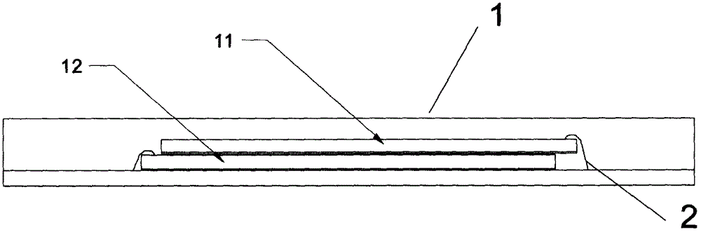
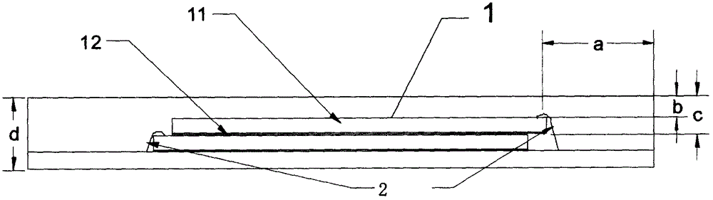
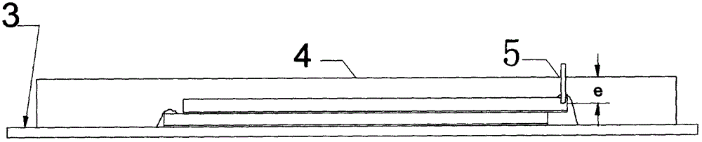
[0025] Such as Figure 1 to Figure 6 As shown, the present invention provides a method of cutting and breaking the package body to realize the degradation of stacked IC defective products, including package outline drawings and internal bonding wire drawings, IC, die, metal wire 2, blade 5, dicing machine, and the IC has A multi-layer structure, which is achieved by the following method,

[0026] First, determine the die of the problematic layer in the internal multi-layer structure of the measured IC through testing;

[0027] Second, determine the cutting position of the cutting knife and set the parameters, the method is as follows:

[0028] Determine the position of the metal wire 2 leading out fr...


PUM

PropertyMeasurementUnit
Blade thicknessaaaaaaaaaa

Abstract

The invention discloses a method for realizing the degradation of stacked IC defective products through cutting the break line of a package body. the method comprises the steps of packaging an outline drawing, an internal weld line drawing, an IC, a die, a metal line, a blade and a scribing machine, wherein the IC is of a multi-layer structure; figuring out a problematic layer die among the internal multi-layer structure of the IC through testing; determining the feeding position of the blade and setting parameters; putting a to-be-cut IC onto the cutting disc of the scribing machine with the vacuum adsorption function by means of the scribing machine for cutting wafers in order to meet the requirements on the cutting precision; cutting to obtain IC particles; cleaning and drying particles in the scribing machine, and testing rest dies after the cleaning and drying process, wherein the ICs of rest dies without problems are adopted as degraded products. According to the technical scheme of the invention, scrapped ICs are degraded and used based on the physical damage isolation method. Therefore, the income is increased, and waste is reduced.

Description

technical field [0001] The invention belongs to the technical field of integrated circuit packaging, and discloses a method for realizing the degradation of stacked IC defective products by cutting and breaking wires in the package. Background technique [0002] In order to increase capacity and increase functions of IC packaging, multi-die (wafer chip) packaging is generally used, which includes multiple die packages placed in parallel and stacked die packages, wherein the number of die stacked layers ranges from 2 to The 16 layers vary. Of course, there are also the same type of die stacked package and different types of die stacked package, so that the higher the integration level, the easier it is for IC users to use; the application of multiple die packages has obvious advantages, but the packaging yield will be lower than For the package of a single die, the ratio of defective products increases exponentially according to the number of superimposed dies. Simply put, a ...

Claims


Application Information

Patent Timeline
IPC IPC(8): H01L21/78H01L21/66
CPCH01L21/78H01L22/12
Inventor 凡会建李文化彭志文
Owner TEKISM
Why Eureka
Try Eureka