Ultraviolet LED optical system for surface curing and manufacturing method thereof
A technology of an optical system and a manufacturing method, which is applied in the field of optical systems for UV LED surface curing, and can solve problems such as poor uniformity of light spots, difficulty in packaging, and difficulty in meeting the requirements of ultraviolet curing for irradiance intensity and uniformity of light spots.
- Summary
- Abstract
- Description
- Claims
- Application Information
AI Technical Summary
Problems solved by technology
Method used
Image
Examples
Embodiment
[0073] A method for manufacturing an ultraviolet LED surface curing optical system, comprising the following steps:
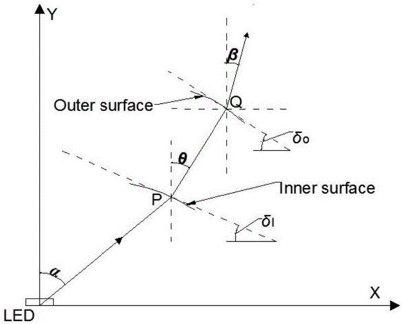
[0074] Step 1: If figure 1 As shown, a plane coordinate system is established with the coordinate origin O(0,0), including the X-axis and Y-axis, and the coordinate origin O is the ultraviolet LED light source. The following are the discrete inner and outer contours of the near-Lambertian LED lens Derivation of point coordinate iterative relationship;
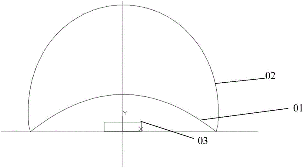
[0075] Production of near-Lambertian LED lens outline;
[0076] The light emitted from the LED chip passes through point P on the inner surface of the lens and point Q on the outer surface of the lens, and undergoes two refractions. It can be seen from the optical theory that when the two deviation angles of the light rays are equal, the phase difference of the lens is the smallest, and it can be obtained:
[0077] θ = α + β ...
PUM
 Abstract
Description
Claims
Application Information


