A method for analyzing data storage structure of nand FLASH memory chip

A data storage and structure analysis technology, applied in the direction of electrical digital data processing, memory address/allocation/relocation, redundant data error detection in operation, etc., can solve the problem of different software solutions and no NANDFLASH memory chip Data storage structure analysis methods and other issues, to achieve the effect of strong versatility and practicability

Active Publication Date: 2020-11-06
中国人民解放军61660部队
View PDF2 Cites 0 Cited by
  • Summary
  • Abstract
  • Description
  • Claims
  • Application Information

AI Technical Summary

Problems solved by technology

[0004] Due to the different page sizes of NAND FLASH, designers have different software solutions, and there is no mature and general method for analyzing the data storage structure of NAND FLASH memory chips in the prior art

Method used


Image

  • A method for analyzing data storage structure of nand FLASH memory chip
  • A method for analyzing data storage structure of nand FLASH memory chip
  • A method for analyzing data storage structure of nand FLASH memory chip

Examples


Embodiment Construction

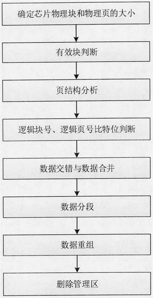
[0031] Specific embodiments of the present invention will be described in detail below in conjunction with the accompanying drawings.

[0032] This embodiment implements a method for analyzing the data storage structure of a NAND FLASH memory chip, such as figure 1 As shown, in order to describe the present invention in detail, the implementation process of this embodiment will be specifically described below by taking a NANDFLASH storage device with a main control chip model of AU6986 and a memory chip model of 29F64G08CAMD2 as an example. It is known that the NAND FLASH storage device includes a storage chip, and the data in the chip is stored in the form of the file system FAT32. The specific implementation process of analyzing the data structure of the chip is as follows:

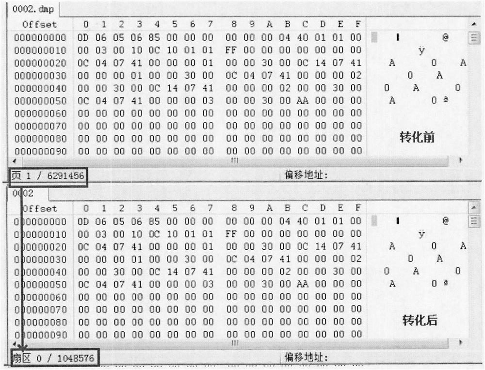
[0033] Extract and open the image file: extract the physical image of the NAND FLASH memory chip through the NAND FLASH reading device. The memory chip includes two wafers inside, so the obtained physi...


PUM


Abstract

The invention discloses a data storage structure analyzing method of a NAND FLASH memory chip. The method comprises: determining the size of physical blocks and the size of physical pages of the chip, and opening a physical image as read-only; carrying out valid block judgement; analyzing the structure of the pages by utilizing the physical pages where continuous data exists; determining the positions of logical block numbers and the positions of logical page numbers according to the changes over bits of each physical page admin area; conducting data interleave analyzing and data merging according to the data continuity condition of a data volume which can reflect the continuity about data; judging whether or not to conduct data segmenting according to the duplication of the logical block numbers; conducting data reorganizing; and deleting the admin area data, and finally obtaining a logical image file. According to the data storage structure analyzing method of the NAND FLASH memory chip, the conversion from the physical image to the logical image of the storage chip is realized on the premise that an NAND FLASH control circuit is not used, thus the aim that conducting data recovering and obtaining evidence after this class of devices are damaged is achieved.

Description

technical field [0001] The invention belongs to the technical field of NAND FLASH storage devices, in particular to a method for analyzing the data storage structure of a NAND FLASH storage chip. Background technique [0002] As a new generation of semiconductor memory, storage devices based on NAND FLASH are widely used in the field of electronic products. The reading and writing unit of block devices such as traditional hard disks is a sector, but the reading and writing characteristics of NAND FLASH storage devices are different. Generally, a NAND FLASH storage device includes at least one NAND FLASH chip, each chip includes at least one wafer, each wafer consists of several blocks, and each block includes several pages. The operation unit of NAND erasing is block, and the operation unit of writing is page, and the same memory location cannot be repeatedly written. It must be erased before writing. In order to avoid frequent "erase-write" operations affecting the perfor...

Claims


Application Information

Patent Timeline
Patent Type & Authority Patents(China)
IPC IPC(8): G06F11/14G06F12/02
CPCG06F11/1448G06F12/02
Inventor 袁建国管乐乐林晨王凯旋张曦高岩连海港李杰白红军王晓海刘永刚于学荣蒋铭卢罡王健
Owner 中国人民解放军61660部队
Why Eureka
Try Eureka