Pixel circuit, driving method of pixel circuit and related devices

A technology of pixel circuit and drive transistor, which is applied to instruments, static indicators, etc., and can solve problems affecting image display effect, uneven display brightness, uneven brightness, etc.

Active Publication Date: 2016-12-07
BOE TECH GRP CO LTD
View PDF11 Cites 20 Cited by
  • Summary
  • Abstract
  • Description
  • Claims
  • Application Information

AI Technical Summary

Problems solved by technology

Due to reasons such as process technology and device aging, the threshold voltage V of the driving transistor of the pixel circuit will be th There is inhomogeneity, which causes the current flowing through each OLED to change, making the display brightness uneven, which affects the display effect of the entire image
And because the current flowing through each OLED is related to the source of the driving tube, that is, the power supply voltage, the current difference in different regions will also be caused due to IRDrop, which will cause uneven brightness of OLEDs in different regions.

Method used


Image

  • Pixel circuit, driving method of pixel circuit and related devices
  • Pixel circuit, driving method of pixel circuit and related devices
  • Pixel circuit, driving method of pixel circuit and related devices

Examples


Embodiment 1

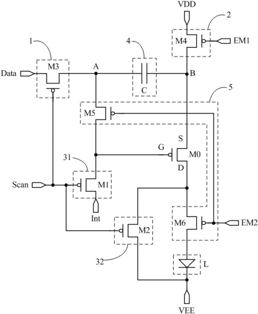
[0097] Such as Figure 2a As shown, the driving transistor M0 is a P-type transistor, and all switching transistors are P-type transistors; each switching transistor is turned off under the action of a high level, and turned on under the action of a low level; the corresponding input timing diagram is as follows Figure 3a shown. Specifically, choose the Figure 3a The four stages T1, T2, T3 and T4 in the input timing diagram shown.

[0098] In the T1 stage, Scan=0, EM1=0, and EM2=1.

[0099] Because Scan=0, the first switch transistor M1, the second switch transistor M2 and the third switch transistor M3 are all turned on; because EM1=0, the fourth switch transistor M4 is turned on; because EM2=1, the fifth switch Both the transistor M5 and the sixth switching transistor M6 are turned off. The turned-on third switch transistor M3 converts the voltage V of the data signal terminal Data Data Provided to the first node A, that is, the first terminal of the capacitor C, so t...

Embodiment 2

[0108] Such as Figure 2b As shown, the driving transistor M0 is a P-type transistor, and all switching transistors are N-type switching transistors; each switching transistor is turned on under the action of a high level, and is turned off under the action of a low level; the corresponding input timing diagram is as follows Figure 3b shown. Specifically, choose the Figure 3b The four stages T1, T2, T3 and T4 in the input timing diagram shown.

[0109] In the T1 stage, Scan=1, EM1=1, and EM2=0.

[0110] Since Scan=1, the first switch transistor M1, the second switch transistor M2 and the third switch transistor M3 are all turned on; because EM1=1, the fourth switch transistor M4 is turned on; because EM2=0, the fifth switch Both the transistor M5 and the sixth switching transistor M6 are turned off. The turned-on third switch transistor M3 converts the voltage V of the data signal terminal Data Data Provided to the first node A, that is, the first terminal of the capaci...


PUM


Abstract

The invention discloses a pixel circuit, a driving method of the pixel circuit, an organic electroluminescence display panel and a display device. The pixel circuit comprises a data writing-in module, a power supply voltage control module, a breakover control module, a storage module, a light-emitting control module, a driving transistor and a light-emitting device. Through cooperation of the five modules and the driving transistor, the working current, for driving the light-emitting device to emit light, of the driving transistor in the pixel circuit can be only relevant to the voltage at a data signal end and the voltage of an original signal end and be irrelevant to the threshold voltage of the driving transistor and the voltage of a first power supply end, and it can be avoided that the working current flowing across the light-emitting device is influenced by the threshold voltage of the driving transistor and the IR Drop, so that the working current for driving the light-emitting device to emit light is maintained stable, and then the frame brightness uniformity of a display area in a display device is improved.

Description

technical field [0001] The invention relates to the field of display technology, in particular to a pixel circuit, a driving method thereof, an organic electroluminescence display panel and a display device. Background technique [0002] Organic Light Emitting Diode (OLED) is one of the hot spots in the field of flat panel display research today. Compared with Liquid Crystal Display (LCD), OLED display has low energy consumption, low production cost, self-illumination, and wide viewing angle. and quick response. At present, OLED displays have begun to replace traditional LCD displays in display fields such as mobile phones, tablet computers, and digital cameras. [0003] Unlike LCDs that use a stable voltage to control brightness, OLEDs are driven by current and require a stable current to control their light emission. Due to reasons such as process technology and device aging, the threshold voltage V of the driving transistor of the pixel circuit will be th There is inho...

Claims


Application Information

Patent Timeline
Patent Type & Authority Applications(China)
IPC IPC(8): G09G3/3225
CPCG09G3/3225G09G2300/0819G09G2310/0262G09G2320/045G09G3/3233G09G2300/0842G09G2300/0861G09G2310/0251G09G3/3266G09G3/3275G09G2320/0233
Inventor 王志良马占洁
Owner BOE TECH GRP CO LTD
Why Eureka
Try Eureka