Method of testing life cycle of Nand flash
A technology of life cycle, read and write testing, applied in static memory, instruments, etc., can solve the problem of lengthy time spent, and achieve the effect of reducing the number of read/write/erase blocks and reducing the test time
- Summary
- Abstract
- Description
- Claims
- Application Information
AI Technical Summary
Problems solved by technology
Method used
Image
Examples
Embodiment
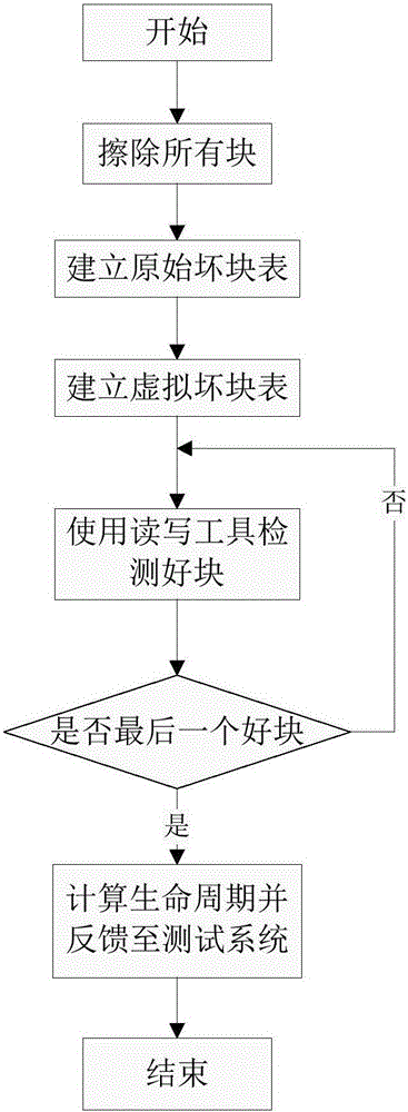
[0031] Please refer to image 3 , the embodiment of the present invention is a kind of method of testing Nand flash life cycle, specifically comprises the following steps:
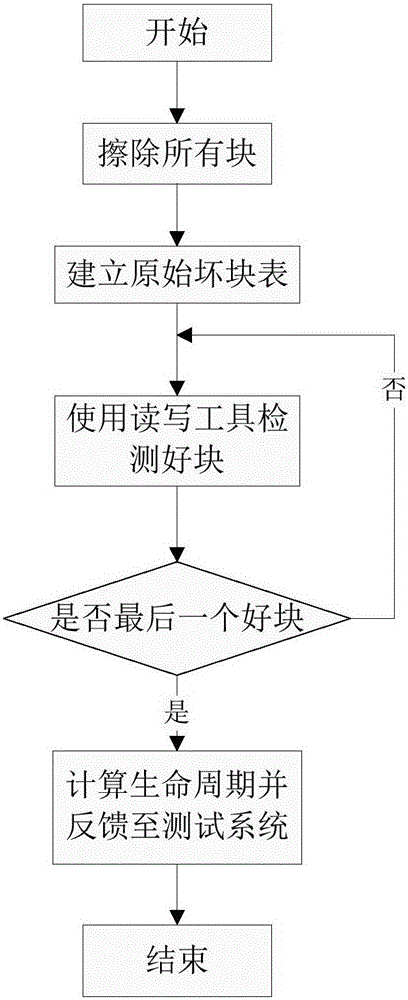
[0032] (1) all blocks are erased, and an original bad block table is set up, wherein the original bad block table is scanned and generated according to prior art methods;
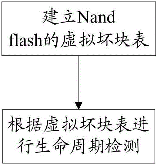
[0033] (2) set up a virtual bad block table at the tool end, the tool end refers to the mass production tool such as in the windows system, and the mass production tool is the card opening tool running on the computer, such as the card opening tool of the U disk , the virtual bad block table is a sequence of bad blocks randomly generated by the system, the total number of these virtual bad blocks is greater than the number of bad blocks in the original bad block table, and the virtual bad blocks include all The data is written into the real bad block to affect the test result. The number of bad blocks in the virtual bad block table ca...
PUM
 Abstract
Description
Claims
Application Information
 - R&D
- Intellectual Property
- Life Sciences
- Materials
- Tech Scout
- Unparalleled Data Quality
- Higher Quality Content
- 60% Fewer Hallucinations
Browse by: Latest US Patents, China's latest patents, Technical Efficacy Thesaurus, Application Domain, Technology Topic, Popular Technical Reports.
© 2025 PatSnap. All rights reserved.Legal|Privacy policy|Modern Slavery Act Transparency Statement|Sitemap|About US| Contact US: help@patsnap.com


