

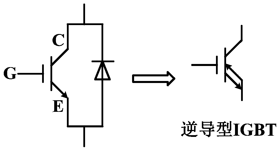
A kind of reverse conduction igbt
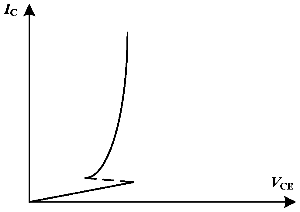
A reverse-conducting, N-type technology, applied in the field of power semiconductor devices, to eliminate the negative resistance effect and improve the forward and reverse conduction performance.
- Summary
- Abstract
- Description
- Claims
- Application Information
AI Technical Summary
Problems solved by technology
Method used
Image

Examples
Embodiment 1
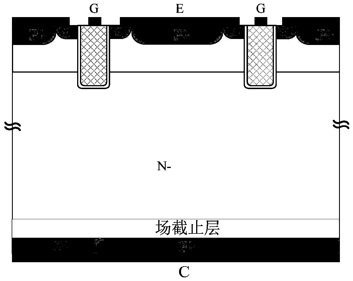
[0019] Example 1, such as Figure 4 As shown, this example is a trench gate reverse conduction IGBT. P-type regions 1 are formed on the surface of the N-type high-resistance semiconductor material, and N-type emitter regions 3 and P-type body contact regions 4 are alternately formed on the surface of the P-type regions along the lateral direction of the device. In the middle of the N-type emitter region 3, a dielectric groove 2 is formed that runs through the P-type region and is in contact with the N-type high-resistance semiconductor at the bottom. The dielectric groove is composed of an insulating dielectric layer 21 located on the inner wall of the groove and a conductive material 22 surrounded by the insulating dielectric layer. The gate electrode is led out from the conductive material in the dielectric groove to form a groove gate structure; the common leading end of the N-type emitter region and the P-type body contact region is the emitter electrode. On the back of t...
Embodiment 2
[0023] Such as Figure 5 As shown, this example is a trench gate reverse conduction IGBT. The difference between this example and Example 1 is that the widths of the heavily doped N-type regions in the electric field stop region 6 along the lateral direction of the device are equal, and the lightly doped P-type regions in the electric field stop region 6 The width along the lateral direction of the device is not equal (ΔL 1 , ΔL 2 , ΔL 3 , ΔL 4 , ΔL 5 ).
Embodiment 3
[0025] Such as Figure 6 As shown, this example is a planar gate reverse conduction IGBT. Several P-type well regions 1 are formed on the surface of the N-type high-resistance semiconductor material, and an N-type emitter region 3 and a P-type body contact region 4 are formed side by side on the surface of the P-type well region along the device lateral direction, and the N-type emitter region is close to the P-type well The P-type body contact region is far away from the edge of the P-type well region, and the common lead end of the two is the emitter electrode, and the N-type emitter region has a distance from the edge of the P-type well region. The semiconductor surface between two adjacent N-type emitter regions 3 in two adjacent P-type well regions is covered with a gate dielectric, and the surface of the gate dielectric is covered with conductive material to form a planar gate structure, and a gate electrode is drawn out. On the back of the N-type high-resistance semico...
PUM
 Abstract
Description
Claims
Application Information