Supercharge Your Innovation With Domain-Expert AI Agents!

A Self-Driven Anode Assisted Gate Lateral Insulated Gate Bipolar Transistor

A bipolar transistor, self-driven technology, applied in the direction of semiconductor devices, electrical components, circuits, etc., can solve the problems of complex external drive circuits, weak forward conduction ability of devices, large additional design area, etc., to reduce costs and improve Current conduction capability, effect of reducing additional design area

Active Publication Date: 2019-11-12
CHONGQING UNIV
View PDF3 Cites 0 Cited by
  • Summary
  • Abstract
  • Description
  • Claims
  • Application Information

AI Technical Summary

Problems solved by technology

[0008] The purpose of the present invention is to solve the problems in the prior art that the forward conduction capability of the device is weak, a complex external drive circuit is required, and a large additional design area is required.

Method used


Image

  • A Self-Driven Anode Assisted Gate Lateral Insulated Gate Bipolar Transistor
  • A Self-Driven Anode Assisted Gate Lateral Insulated Gate Bipolar Transistor
  • A Self-Driven Anode Assisted Gate Lateral Insulated Gate Bipolar Transistor

Examples


Embodiment 1

[0055] The first conductivity type is selected as N type, and the second conductivity type is selected as P type.

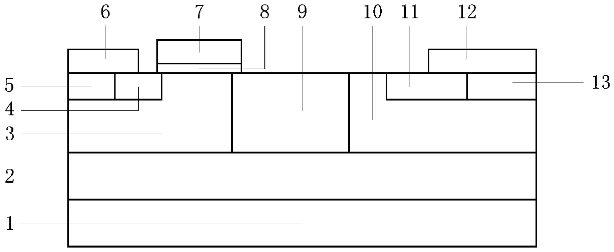
[0056] Such as Figure 6 As shown, a self-driven anode-assisted gate lateral insulated gate bipolar transistor is characterized in that it includes a P-type substrate layer 1, an insulating dielectric layer 2, a P-type cathode well region 3, an N+-type cathode region 4, and a P+-type cathode Area 5, cathode contact area 6, gate contact area 7, gate dielectric layer 8, N-type drift area 9, N-type anode buffer zone 10, P+ type anode area 11, anode contact area 12, N+ type anode area 13, P-type anode well region 17 , anode self-driving gate dielectric layer 18 and anode self-driving gate contact region 19 .

[0057] The P-type substrate layer 1, insulating dielectric layer 2 and N-type drift region 9 constitute an SOI substrate.

[0058] The insulating dielectric layer 2 covers the P-type substrate layer 1 . The P-type substrate layer 1 is doped silicon, and its ...

Embodiment 2

[0073] The first conductivity type is selected as N type, and the second conductivity type is selected as P type.

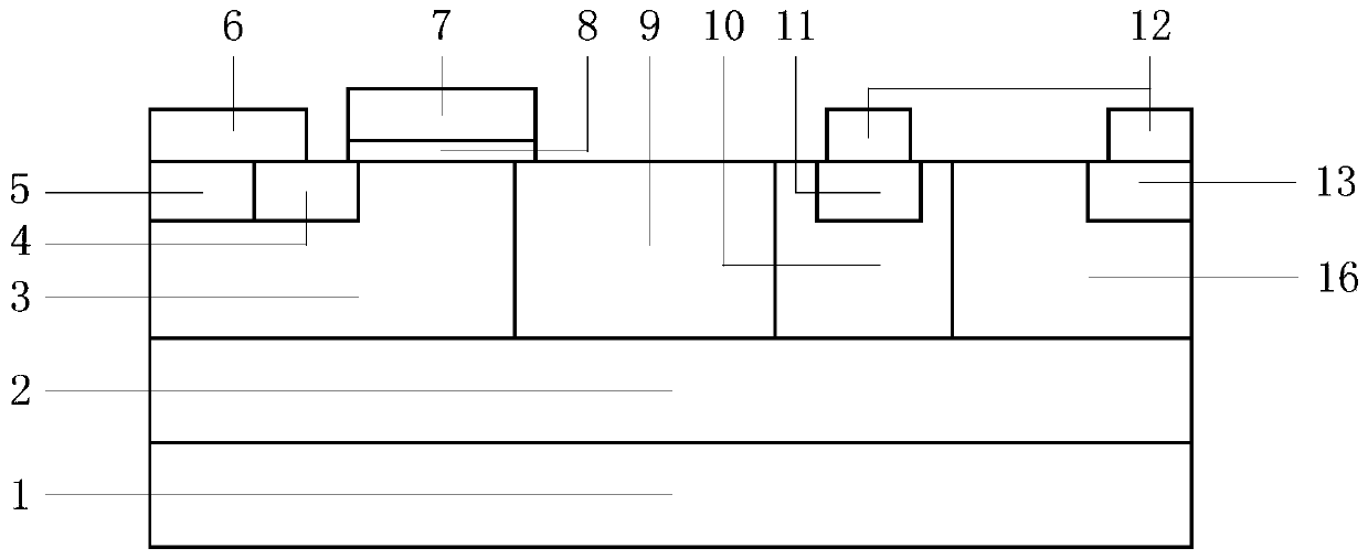
[0074] Such as Figure 7 As shown, a self-driven anode-assisted gate lateral insulated gate bipolar transistor is characterized in that it includes a P-type substrate layer 1, an insulating dielectric layer 2, a P-type cathode well region 3, an N+-type cathode region 4, and a P+-type cathode Area 5, cathode contact area 6, gate contact area 7, gate dielectric layer 8, N-type drift area 9, N-type anode buffer zone 10, P+ type anode area 11, anode contact area 12, N+ type anode area 13, P-type anode well region 17 and anode self-driving gate dielectric layer 18 .

[0075] The P-type substrate layer 1, insulating dielectric layer 2 and N-type drift region 9 constitute an SOI substrate.

[0076] The insulating dielectric layer 2 covers the P-type substrate layer 1 . The P-type substrate layer 1 is doped silicon, and its thickness and impurity concentration have a ...

Embodiment 3

[0090] The first conductivity type is selected as N type, and the second conductivity type is selected as P type.

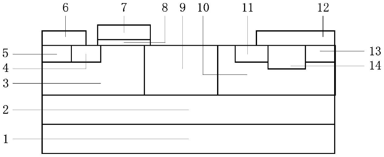
[0091] Such as Figure 8As shown, a self-driven anode-assisted gate lateral insulated gate bipolar transistor includes: a P-type substrate layer 1, an insulating dielectric layer 2, a P-type cathode well region 3, an N+ type cathode region 4, a P+ type cathode region 5, and a cathode Contact area 6, gate contact area 7, gate dielectric layer 8, N-type drift area 9, N-type anode buffer zone 10, P+ type anode area 11, anode contact area 12, N+ type anode area 13, P-type anode well region 17 , anode self-driving gate dielectric layer 18 and anode self-driving gate contact region 19 .

[0092] The insulating dielectric layer 2 covers the P-type substrate layer 1; the P-type substrate layer 1 is doped silicon, and its thickness and impurity concentration have a very wide selection range; the insulating dielectric layer 2 is 0.5 μm- For silicon dioxide with a thickne...


PUM


Abstract

The present invention discloses a self-driven anode auxiliary gate type lateral insulated gate bipolar transistor. The self-driven anode auxiliary gate type lateral insulated gate bipolar transistor comprises an SOI as a substrate and the design structure of a self-driven anode auxiliary gate is adopted. On the premise that the turn-off time of a device is guaranteed to be short, the negative resistance effect of the device during the conduction process is eliminated. The operation stability of the device is improved. In addition, the device is realized through adopting the existing conventional integrated circuit manufacturing process. In this way, the prepared device is reduced in lateral dimension, and the current conduction capability is improved.

Description

technical field [0001] The invention relates to a conductance modulation high-voltage power device in the technical field of semiconductor power electronic devices, in particular to a self-driven anode auxiliary gate lateral insulated gate bipolar transistor. Background technique [0002] Lateral Insulated Gate Bipolar Transistor (LIGBT: Lateral Insulated Gate Bipolar Transistor) made of SOI: Silicon On Insulator (SOI: Silicon On Insulator) as the substrate material, referred to as SOI-LIGBT, especially thin silicon layer SOI-LIGBT, is SOI A key component of high-voltage integrated circuits, it has the advantages of simple driving, large current capability, and easy integration, but its turn-off speed is much faster than that of lateral double-diffused metal-oxide-semiconductor effect transistors (LDMOS, Lateral Double-diffused MOSFET) The slow turn-off speed of the SOI leads to a large switching loss, which affects the application of SOI lateral insulated gate bipolar trans...

Claims


Application Information

Patent Timeline
Patent Type & Authority Patents(China)
IPC IPC(8): H01L29/739H01L29/45H01L29/08
CPCH01L29/0804H01L29/45H01L29/7394
Inventor 陈文锁廖瑞金蒲贤洁曾正邵伟华李辉
Owner CHONGQING UNIV
Features
  • R&D
  • Intellectual Property
  • Life Sciences
  • Materials
  • Tech Scout
  • Unparalleled Data Quality
  • Higher Quality Content
  • 60% Fewer Hallucinations
Learn More