Supercharge Your Innovation With Domain-Expert AI Agents!

A self-driven anode assisted gate insulated gate bipolar transistor

A bipolar transistor, auxiliary gate technology, applied in semiconductor devices, electrical components, circuits, etc., can solve the problems of complex external driving circuits, weak forward conduction capability of devices, etc., to eliminate negative resistance effects and improve working stability. , the effect of small off-time

Active Publication Date: 2020-06-23
CHONGQING UNIV
View PDF2 Cites 0 Cited by
  • Summary
  • Abstract
  • Description
  • Claims
  • Application Information

AI Technical Summary

Problems solved by technology

[0008] The purpose of the present invention is to solve the problems in the prior art, such as weak forward conduction ability of the device and the need for a complex external drive circuit, to obtain an optimized compromise between the on-state loss and the off-state loss

Method used


Image

  • A self-driven anode assisted gate insulated gate bipolar transistor
  • A self-driven anode assisted gate insulated gate bipolar transistor
  • A self-driven anode assisted gate insulated gate bipolar transistor

Examples


Embodiment 1

[0047] The first conductivity type is selected as N type, and the second conductivity type is selected as P type.

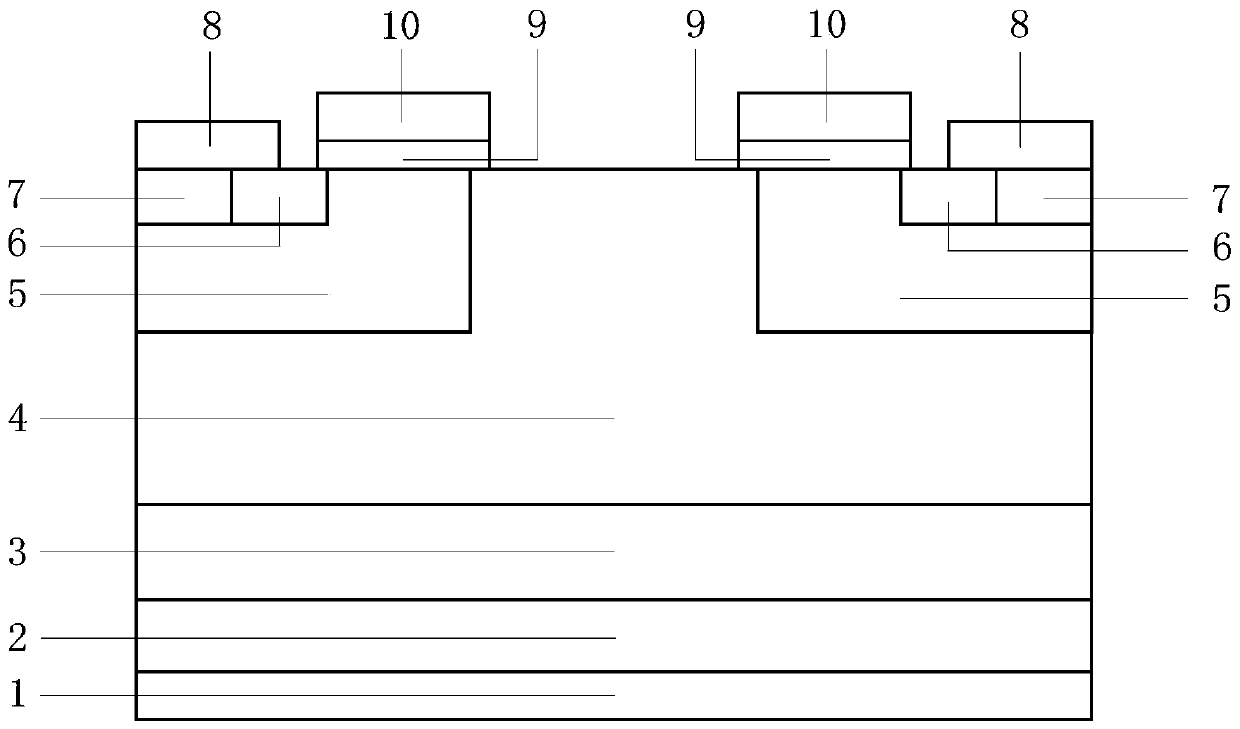
[0048] Such as Figure 4As shown, a self-driven anode assisted gate insulated gate bipolar transistor is characterized in that it includes an anode contact area 1, a P+ type anode area 2, an N type anode buffer area 3, an N type drift area 4, and a P type cathode well Area 5, N+ type cathode area 6, P+ type cathode area 7, cathode contact area 8, gate dielectric layer 9, gate contact area 10, P type anode well area 11, N+ type anode area 12, anode auxiliary gate dielectric layer 13 and the anode auxiliary gate contact region 14.

[0049] The N-type drift region 4 covers the N-type anode buffer zone 3 .

[0050] The P-type cathode well region 5 covers part of the surface above the N-type drift region 4 .

[0051] The N+ type cathode region 6 and the P+ type cathode region 7 cover part of the surface above the P type cathode well region 5 .

[0052] The cathode...
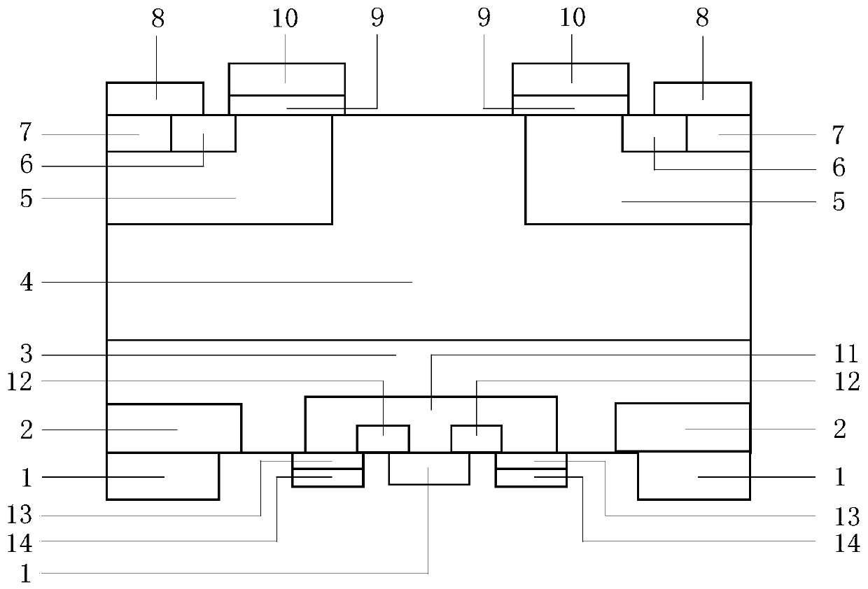
Embodiment 2

[0062] The first conductivity type is selected as N type, and the second conductivity type is selected as P type.

[0063] Such as Figure 5 As shown, a self-driven anode assisted gate insulated gate bipolar transistor is characterized in that it includes an anode contact area 1, a P+ type anode area 2, an N type anode buffer area 3, an N type drift area 4, and a P type cathode well Region 5, N+ type cathode region 6, P+ type cathode region 7, cathode contact region 8, gate dielectric layer 9, gate contact region 10, P type anode well region 11, N+ type anode region 12 and anode auxiliary gate dielectric layer 13.

[0064] The N-type drift region 4 covers the N-type anode buffer zone 3 .

[0065] The P-type cathode well region 5 covers part of the surface above the N-type drift region 4 .

[0066] The N+ type cathode region 6 and the P+ type cathode region 7 cover part of the surface above the P type cathode well region 5 .

[0067] The cathode contact region 8 covers the ...


PUM


Abstract

The invention discloses a rapid insulated gate bipolar transistor. By adoption of an anode self-driven auxiliary gate design structure, a negative resistance effect in electrification of a device can be eliminated on the premise of short power-off time of the device, operation stability of the device is improved, and a great trade-off relation between power-on loss and power-off loss can be obtained. In addition, by a self-driven design of the anode auxiliary gate structure, the requirement of a conventional auxiliary gate electrode anode structure which requires extra drive circuits can be eliminated.

Description

technical field [0001] The invention relates to a conductance modulation high-voltage power device in the technical field of semiconductor power electronic devices, in particular to a self-driven anode auxiliary gate insulated gate bipolar transistor. Background technique [0002] Insulated gate bipolar transistor (IGBT: LateralInsulatedGateBipolarTransistor) has the advantages of simple driving, large current capability, and high withstand voltage capability, but its turn-off speed is much faster than that of double-diffused metal-oxide-semiconductor effect transistors (DMOS, Double-diffusedMOSFET) The slow turn-off speed of the transistor leads to a large switching loss, which affects the application of edge-gate bipolar transistors in power electronic systems. [0003] There are three main methods to increase the turn-off speed of IGBT devices to reduce switching losses: [0004] One is to reduce the lifetime of non-equilibrium carriers in the drift region and increase t...

Claims


Application Information

Patent Timeline
Patent Type & Authority Patents(China)
IPC IPC(8): H01L29/739
CPCH01L29/7395
Inventor 陈文锁蒲贤洁廖瑞金曾正邵伟华李辉
Owner CHONGQING UNIV
Features
  • R&D
  • Intellectual Property
  • Life Sciences
  • Materials
  • Tech Scout
  • Unparalleled Data Quality
  • Higher Quality Content
  • 60% Fewer Hallucinations
Learn More