Method for manufacturing quantum dot display device and corresponding quantum dot display device

A technology of display devices and quantum dots, which is applied in the fields of instruments, printing, optics, etc., can solve the problems of increasing the production cost of quantum dot films, the difficulty of the process, the agglomeration of quantum dot materials, and the complexity of the process.

Active Publication Date: 2016-12-14
BOE TECH GRP CO LTD +1
View PDF17 Cites 3 Cited by
  • Summary
  • Abstract
  • Description
  • Claims
  • Application Information

AI Technical Summary

Problems solved by technology

However, such a special package will inevitably increase the production cost of the quantum dot film and the corresponding process difficulty
In addition, epitaxial technology generally requires relatively expensive equipment, and the process is relatively complicated, so it is not suitable for large-scale industrial production
To sum up, the processing methods for quantum dot materia

Method used


Image

  • Method for manufacturing quantum dot display device and corresponding quantum dot display device
  • Method for manufacturing quantum dot display device and corresponding quantum dot display device
  • Method for manufacturing quantum dot display device and corresponding quantum dot display device

Examples


Embodiment Construction

[0019] The quantum dot display device provided by the embodiments of the present invention and its manufacturing method will be described in detail below with reference to the accompanying drawings. It should be noted that the drawings are not necessarily to scale, emphasis instead generally being placed upon illustrating the principles of the invention. Therefore, the size, position, etc. of each element, film layer, etc. shown in the drawings do not represent the real size, position, etc., and the purpose is only to facilitate the understanding of the realization and principle of the present invention.

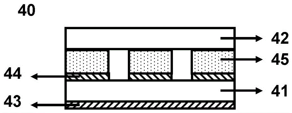
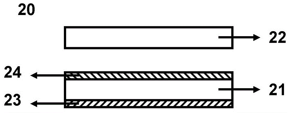
[0020] According to one aspect, an embodiment of the present invention provides a method for manufacturing a quantum dot display device. Specifically, refer to figure 1 and 2 ,in figure 1 is a schematic flowchart illustrating such a manufacturing method, and figure 2 is a schematic cross-sectional view showing a quantum dot display device manufactured by such a manufact...


PUM


Abstract

The invention relates to the technical field of quantum dot displaying and discloses a method for manufacturing a quantum dot display device. The method comprises: providing an array substrate and a butting substrate facing each other; printing alignment solution containing quantum dot material to one side of the array substrate which faces the butting substrate; removing a solvent in the alignment solution printed to the side of the array substrate which faces the butting substrate; after the solvent is removed, heating the array substrate; providing a backlight module on the side of the array substrate which is opposite to the butting substrate. The invention also discloses a corresponding quantum dot display device. By the aid of such manufacturing method, the display quality of the manufactured quantum dot display device is greatly improved, and related manufacture cost and process difficulty are decreased.

Description

technical field [0001] The present invention relates to the technical field of quantum dot display, and in particular to a method for manufacturing a quantum dot display device and a corresponding quantum dot display device. Background technique [0002] With the rapid development of the display field, quantum dot display technology has attracted more and more attention due to its unique luminous properties, excellent stability, wider color gamut coverage, and relatively low cost. Currently, in display devices using quantum dot display technology, the blue light emitted by the backlight is usually used to excite the quantum dot material to emit red light and green light, thereby providing color display. In essence, a quantum dot display device is a device that realizes color display by means of the backlight source and the photoluminescence effect of quantum dot materials. [0003] In the existing quantum dot display devices, the quantum dot material is usually made into a ...

Claims


Application Information

Patent Timeline
IPC IPC(8): G02F1/1333G02F1/13357
CPCG02F1/1333G02F1/1336G02F1/133614G02F2202/108G02F1/133723G02F1/133617B41F3/28G02F2202/36G02F1/133382
Inventor 邢伟强王永茂邓金阳毛振华游洪超罗明
Owner BOE TECH GRP CO LTD
Why Eureka
Try Eureka