Check patentability & draft patents in minutes with Patsnap Eureka AI!

Encapsulation shell and electronic component using the encapsulation shell

A technology for encapsulating shells and electrode layers, applied in the fields of semiconductors, communications, and microelectronics, can solve the problems of unallowable changes in size, additional costs, and limited changes in capacitance values, avoiding additional capital costs, improving progress, and avoiding time costs. Effect

Active Publication Date: 2019-03-12
DYNAX SEMICON
View PDF4 Cites 0 Cited by
  • Summary
  • Abstract
  • Description
  • Claims
  • Application Information

AI Technical Summary

Problems solved by technology

Among them, for changing the capacitance by changing the bonding wire, due to the limitation of the physical size of the package, the amount of change in the capacitance value is limited
The capacitance is changed by changing the size of the package, and the change of the size of the package will cause the length and arc of the bonding wire to change, thereby affecting the matching design of RF microwave devices.
At the same time, the change of package shell size will also cause various mold costs in the shell manufacturing process, and will also cause additional packaging costs and application costs for assembling RF microwave devices to external heat sinks
[0003] In addition, in practical applications, the packages of RF and microwave devices often require the use of some standard model sizes, so changing the capacitance value by changing the bonding wire has certain limitations, and changing the capacitance value by changing the size of the package will cause Bringing matching design and additional cost in terms of electrical performance
In addition, some cases require a standard model size package case whose dimensions are not allowed to change

Method used


Image

  • Encapsulation shell and electronic component using the encapsulation shell
  • Encapsulation shell and electronic component using the encapsulation shell
  • Encapsulation shell and electronic component using the encapsulation shell

Examples


Embodiment Construction

[0027] In order to make the purpose, technical solutions and advantages of the embodiments of the present invention clearer, the technical solutions in the embodiments of the present invention will be clearly and completely described below in conjunction with the drawings in the embodiments of the present invention. Obviously, the described embodiments It is a part of embodiments of the present invention, but not all embodiments. The components of the embodiments of the invention generally described and illustrated in the figures herein may be arranged and designed in a variety of different configurations.

[0028] Accordingly, the following detailed description of the embodiments of the invention provided in the accompanying drawings is not intended to limit the scope of the claimed invention, but merely represents selected embodiments of the invention. Based on the embodiments of the present invention, all other embodiments obtained by persons of ordinary skill in the art wi...


PUM


Abstract

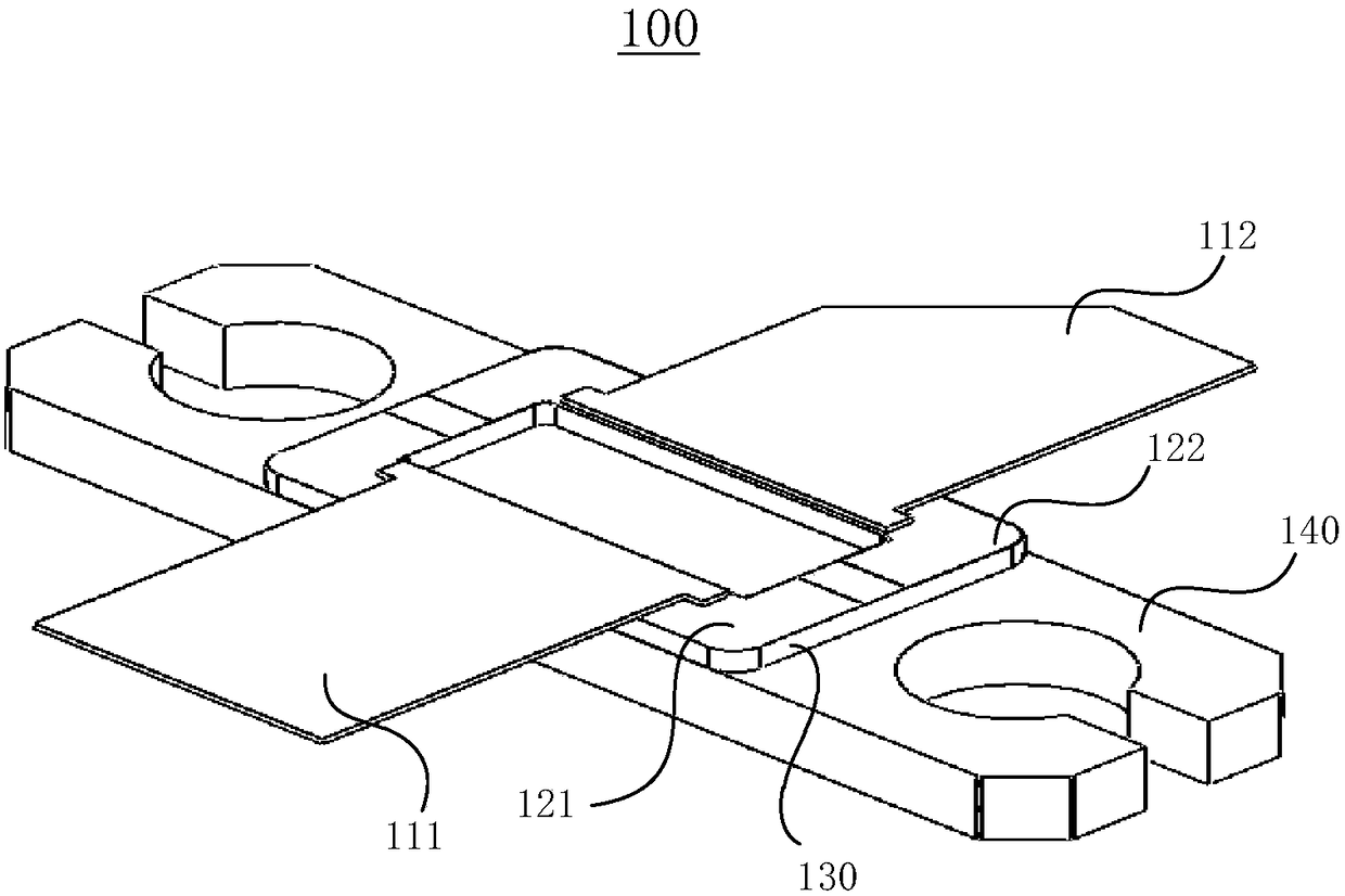
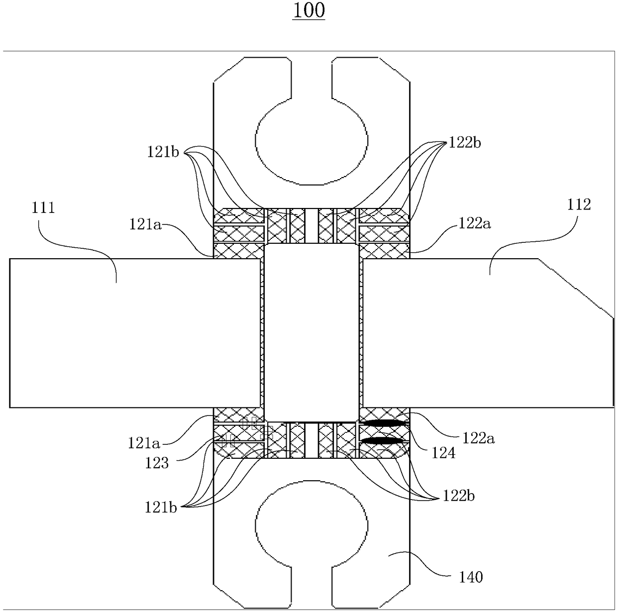
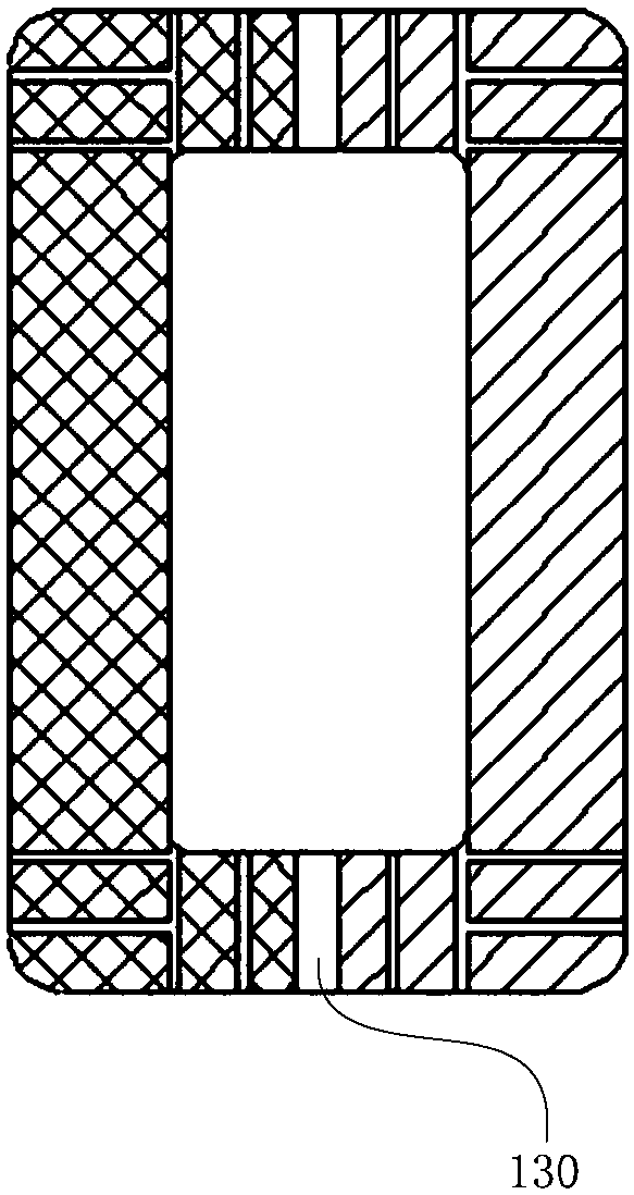
The present invention relates to the fields of microelectronics, semiconductors and communications, in particular to a packaging shell, which includes input leads, output leads, metallized electrode layers for input leads, metallized electrode layers for output leads, walls and metal substrates , the wall is set on the metal substrate, the input lead metallized electrode layer and the output lead metallized electrode layer are arranged on the wall at intervals, the input lead is electrically connected to the input lead metallized electrode layer, the output lead The leads are electrically connected to the output lead metallization electrode layer, and at least one of the input lead metallization electrode layer and the output lead metallization electrode layer includes a plurality of independently arranged metallization areas, and each metallization area is spaced apart from each other. During the use of the package shell, the purpose of adjusting the capacitance value of the package shell is realized by changing the area of ​​the metallized electrode layer of the input or output lead.

Description

technical field [0001] The invention relates to the fields of microelectronics, semiconductors and communications, in particular to a package shell and an electronic component using the package shell. Background technique [0002] Radio frequency and microwave technology have been widely used in communication systems and radar systems. Capacitance and inductance in radio frequency microwave design directly affect the performance of the entire circuit. Typically, the way to control the capacitance value is by changing the length and arc of the bonding wire or the size of the package case. For changing the capacitance by changing the bonding wire, the amount of change in the capacitance value is limited due to the limitation of the physical size of the package shell. The capacitance is changed by changing the size of the package, and the change of the size of the package will cause the length and arc of the bonding wire to change, thereby affecting the matching design of the ...

Claims


Application Information

Patent Timeline
Patent Type & Authority Patents(China)
IPC IPC(8): H01L23/043
CPCH01L23/043H01L2224/49111H01L2224/49175
Inventor 杨琼
Owner DYNAX SEMICON
Features
  • R&D
  • Intellectual Property
  • Life Sciences
  • Materials
  • Tech Scout
  • Unparalleled Data Quality
  • Higher Quality Content
  • 60% Fewer Hallucinations
Learn More