
Touch screen copper wiring method ad touch screen

A touch screen, metal copper technology, applied in semiconductor/solid-state device manufacturing, input/output process of data processing, instruments, etc., can solve the problems of poor touch screen operation, poor display quality, etc. Excellent, the display quality is fresh, the effect of low resistance

Inactive Publication Date: 2017-01-04
EELY ECW TECH
View PDF4 Cites 0 Cited by
  • Summary
  • Abstract
  • Description
  • Claims
  • Application Information

AI Technical Summary

Problems solved by technology

[0003] In view of the above-mentioned problems existing in the prior art, the purpose of the present invention is to provide a touch screen copper process method and a touch screen to solve the existing problems of poor touch screen operation and unclear display quality.

Method used


Image

  • Touch screen copper wiring method ad touch screen
  • Touch screen copper wiring method ad touch screen

Examples


Embodiment Construction

[0044] The following will clearly and completely describe the technical solutions in the embodiments of the present invention with reference to the accompanying drawings in the embodiments of the present invention. Obviously, the described embodiments are only some, not all, embodiments of the present invention. Based on the embodiments of the present invention, all other embodiments obtained by persons of ordinary skill in the art without making creative efforts belong to the protection scope of the present invention.

[0045] For the convenience of description, spatially relative terms such as "under", "under", "under", "over", "on" and other spatially relative terms may be used herein to describe an element as shown in the drawings Or the relationship of a feature to another element or feature(s). It will be understood that when an element or layer is referred to as being "on," "connected to," or "coupled to" another element or layer, it can be directly on, directly on, or ...


PUM

PropertyMeasurementUnit
thicknessaaaaaaaaaa

Abstract

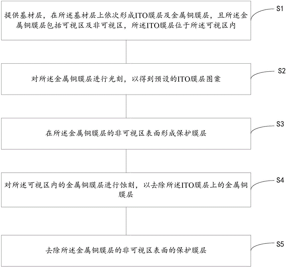
The invention provides a touch screen copper wiring method. The method comprises the following steps of: S1, providing a base material layer, and forming an ITO film layer and a metal copper film layer on the base material layer in sequence, wherein the metal copper film layer comprises a visible area and an invisible area, and the ITO film layer is located in the visible area; S2, photoetching the metal copper film layer to obtain a preset ITO film layer pattern; S3, forming a protection film layer on the surface of the invisible area of the metal copper film layer; S4, etching the metal copper film layer in the visible area so as to remove the metal copper film layer on the ITO film layer; and S5, removing the protection film layer on the surface of the invisible area of the metal copper film layer. According to the touch screen copper wiring method, a manner of carrying out lap joint between Ag and ITO is replaced by a manner of integrally forming the metal copper film layer and the ITO, so that the problem that the precision of the lap joint between the Ag and the ITO is low is solved. Moreover, the invention provides a touch screen prepared by adoption of above copper wiring method.

Description

technical field [0001] The invention relates to the field of touch screen preparation technology, in particular to a touch screen copper manufacturing method and a touch screen. Background technique [0002] At present, touch screens of smart electronic devices usually use Ag (silver) to overlap ITO (indium tin oxide). However, using this method not only has many difficulties in the production process, such as low overlapping accuracy and easy circuit breakage, but also when the When it is applied to smart electronic devices, it is also prone to problems such as poor operating feel, high delay, and insufficient display quality. It cannot meet the user's requirements for the display quality of the touch screen, which greatly reduces the user experience. Contents of the invention [0003] In view of the above-mentioned problems in the prior art, the purpose of the present invention is to provide a touch screen copper manufacturing method and a touch screen to solve the probl...

Claims


Application Information

Patent Timeline
Patent Type & Authority Applications(China)
IPC IPC(8): G06F3/041C23F1/02G03F7/26
CPCG06F3/041G06F3/0412C23F1/02G03F7/26G06F2203/04103
Inventor 宋洪波李均李学才
Owner EELY ECW TECH
Learn More