Method, apparatus and system for accessing flash memory device

A technology for accessing devices and equipment, applied in information storage, static memory, read-only memory, etc., and can solve the problems of storage element storage data misjudgment, data misjudgment, leakage, etc.

Inactive Publication Date: 2017-01-04
HUAWEI TECH CO LTD
View PDF8 Cites 18 Cited by
  • Summary
  • Abstract
  • Description
  • Claims
  • Application Information

AI Technical Summary

Problems solved by technology

[0004] However, in practical applications, since the electrons in the memory cell will leak over time, the threshold voltage of the memory cell will also shift to a lower voltage after the electron leaks, so, using the above method, for storing data 0 memory element, when its threshold voltage Vth shifts to be lower than the preset decision voltage Vread, it will cause misjudgment of the data stored in the memory element; for example, refer to figure 1 , t

Method used


Image

  • Method, apparatus and system for accessing flash memory device
  • Method, apparatus and system for accessing flash memory device
  • Method, apparatus and system for accessing flash memory device

Examples


Embodiment 1

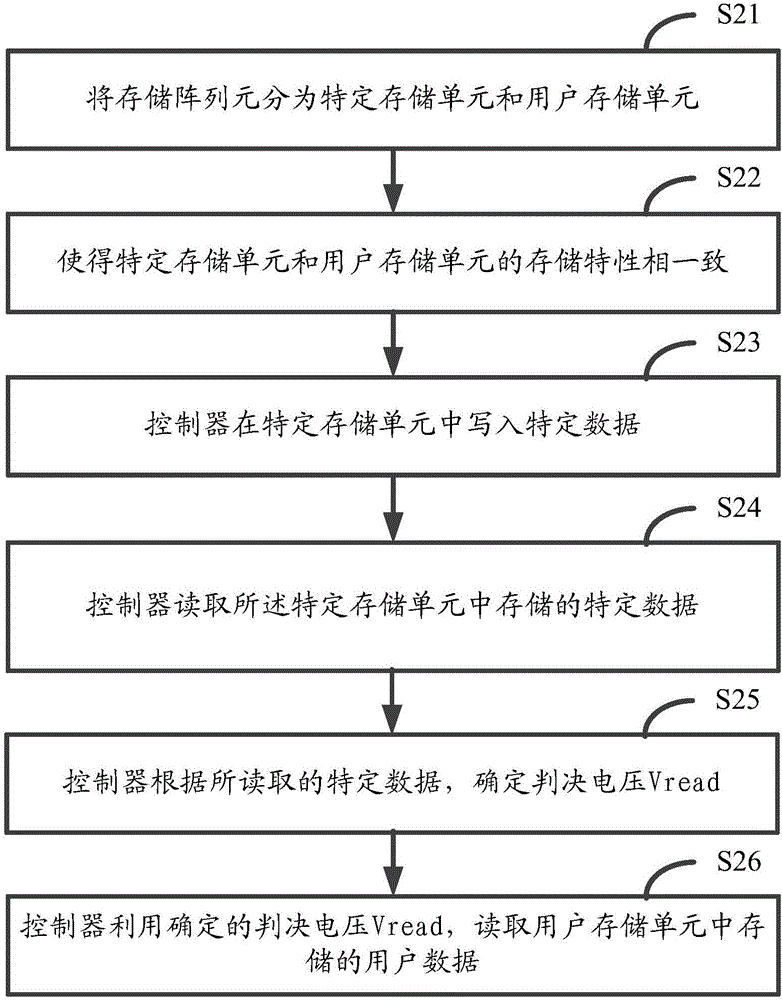
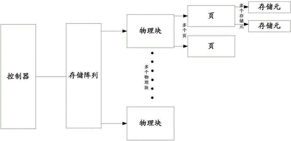
[0053] Based on the above-mentioned application scenario, the present invention provides a method for accessing a flash memory device. The flash memory device can be specifically a U disk (USB flash disk, USB flash disk) and SSD (Solid State Drives, solid state drive) and other devices. The flash memory device can be specifically composed of Controller and storage array are formed, and the function of controller can be realized by control chip specifically, and the function of storage array can be realized by storage chip specifically, and storage chip is Flash chip, and the chip of Flash type can be specifically Nand flash chip; And the present invention provides The access method of the flash memory device, such as figure 2 As shown, the following steps may be specifically included:

[0054] Step S21: first divide the storage array into specific storage units and user storage units;

[0055] Wherein, the specific storage unit is specifically used to store specific data, th...

Embodiment 2

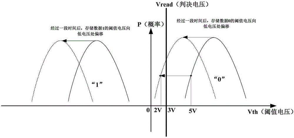
[0072] In the embodiment of the present invention, the step S24 "the controller reads the specific data stored in the specific storage unit" in the first embodiment above may specifically be: the controller obtains the current threshold voltage Vth of the specific storage unit; the controller compares the preset The decision voltage Vread and the current threshold voltage Vth of the specific memory cell determine the specific data stored in the specific memory cell. In the embodiment of the present invention, a specific storage unit may include a plurality of storage elements, and the threshold voltage Vth obtained above may also specifically obtain the threshold voltage Vth of a plurality of storage elements; as before, for an SLC type flash memory device, it may be specifically When the preset decision voltage Vread is greater than the current threshold voltage Vth of the memory cell in the specific memory cell, it is determined that the data stored in the memory cell of the ...

Embodiment 3

[0098] The present invention also provides another access method of a flash memory device, which can be specifically applied to a solid-state hard disk SSD, and the method is specifically as follows:

[0099] First, each physical block in the SSD storage array is allocated a BIT (Block Info Table, physical block information table) in advance, which can record the PE (erasing) times, storage duration (Retention) and Read information such as number of times; Then set a Calibration Table (calibration table), this table uses PE, Retention, number of readings and ambient temperature as index, stores the offset value of the judgment voltage Vread of SSD memory array; Wherein, BIT and CalibrationTable can be It is specifically stored in the storage medium of the SSD controller.

[0100] In the embodiment of the present invention, in order to make the SSD have a certain error correction capability, the data written into the SSD is generally subjected to ECC (Error Correcting Code, err...


PUM


Abstract

The invention discloses a method, an apparatus and a system for accessing a flash memory device. The flash memory device comprises a controller and a storage array, the storage array comprises a specific storage unit and a user storage unit, wherein the specific storage unit is used for storing specific data, the user storage unit is used for storing user data, and the specific data is used for determining a decision voltage for reading the user data. The method comprises the following steps: the controller reads the specific data stored in the specific storage unit, determines the decision voltage according to the read specific data, and reads the user data stored in the user storage unit via the determined decision voltage. By adoption of the method, apparatus and system disclosed by the invention, wrong decision to the data stored in the flash memory device can be reduced.

Description

technical field [0001] The present invention relates to the technical field of data storage, in particular to an access method, device and system for a flash memory device. Background technique [0002] The flash memory device is a long-life non-volatile storage array, and the stored data will not be lost even if the power is turned off. Due to the non-volatile storage characteristics and high-speed read and write performance of flash memory devices, they have been widely used in recent years. [0003] In practical applications, the smallest storage unit of a flash memory device is a storage unit, and data is stored in the form of electrons in the storage unit, and different data are represented by different threshold voltages Vth in the storage unit; for example, in a single In a memory array of the single-level cell (SLC, Single-level cell) type, each memory cell stores one bit of data, and the stored data is 0 or 1; wherein, as figure 1 As shown, when the storage elemen...

Claims


Application Information

Patent Timeline
IPC IPC(8): G06F3/06
CPCG06F3/0614G06F3/0658G06F3/0679G06F3/06G11C16/28G11C16/3404G11C16/3418G06F3/0619G06F11/1068G11C16/26G11C16/349G11C29/52
Inventor 周冠锋
Owner HUAWEI TECH CO LTD
Why Eureka
Try Eureka