A kind of deep ultraviolet semiconductor light-emitting diode and its preparation method
A technology of light-emitting diodes and semiconductors, applied in semiconductor devices, electrical components, circuits, etc., can solve problems such as complex processes, affecting internal quantum efficiency, and strict process requirements, to overcome strong absorption, improve light extraction efficiency, and simple process reliable effect
- Summary
- Abstract
- Description
- Claims
- Application Information
AI Technical Summary
Problems solved by technology
Method used
Image

Examples
Embodiment 1
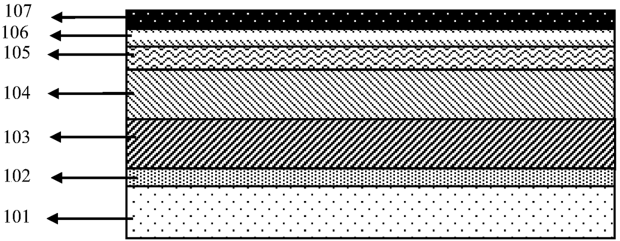
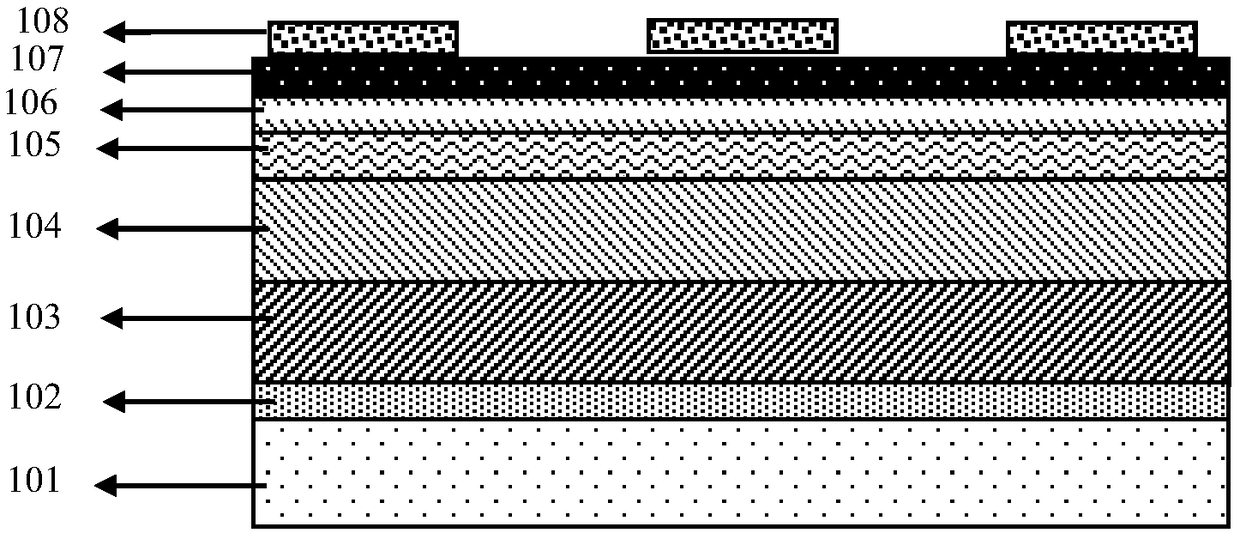
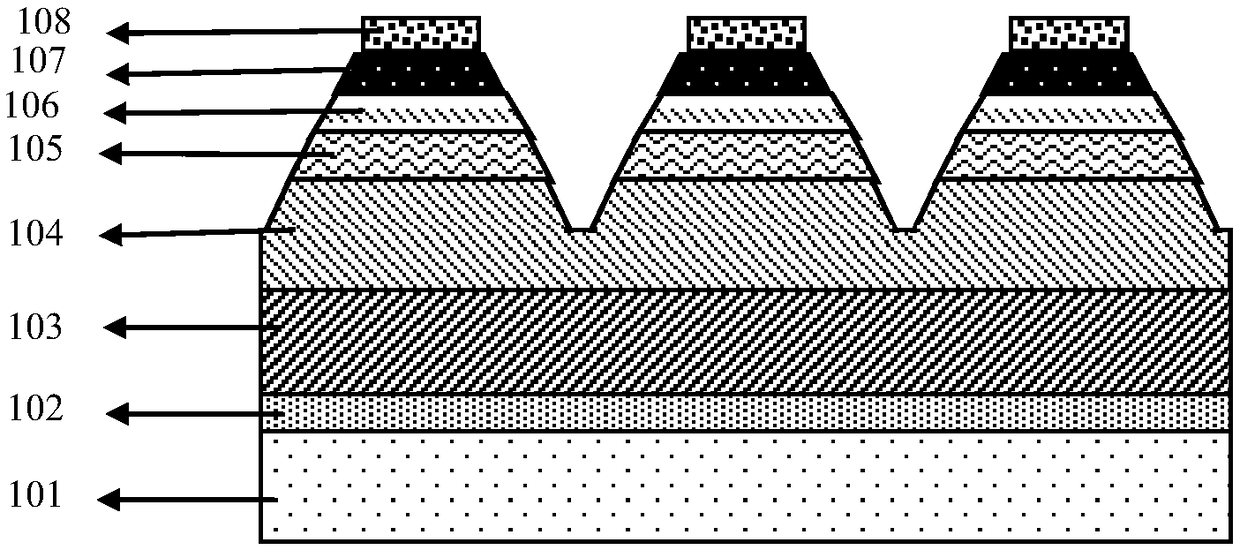
[0054] The DUV LED with the same-side flip-chip structure in this embodiment, from bottom to top, is a sapphire substrate 101, a nucleation layer 102, an undoped aluminum nitride layer 103, an n-type aluminum gallium nitride layer 104, and an n-type aluminum gallium nitride layer. The N-type electrode 201 above the AlGaN layer 104, the active layer 105, the electron blocking layer 106, the p-type hole conduction layer 107, the suspended conductive layer 109 of the graphene layer and the P-type electrode 202; One side of the surface of the p-type hole conduction layer 107 forms a micro-nano structure array with inclined sidewalls, and a suspended conductive layer 109 with a graphene layer is prepared on the top of the micro-nano structure array with inclined sidewalls. Air remains between the micro-nano structures.
[0055] The preparation method of the DUV LED with the same-side flip-chip structure in this embodiment, the steps are as follows:
[0056] The first step, the pre...
Embodiment 2
[0069] The DUV LED with vertical flip-chip structure in this embodiment consists of N-type electrode 201, n-type AlGaN layer 104, active layer 105, electron blocking layer 106, p-type hole conducting layer 107, sulfur The suspended conductive layer 109 of the molybdenum layer and the P-type electrode 202 are formed; on the surface side of the p-type hole conduction layer 107 of the epitaxial sheet, a micro-nano structure array with inclined sidewalls is formed, and the micro-nano structure array of inclined sidewalls A suspended conductive layer 109 with a molybdenum sulfide layer is prepared on the top, and air is kept between the micro-nano structures with inclined side walls.
[0070] The preparation method of the DUV LED with the same-side flip-chip structure in this embodiment, the steps are as follows:
[0071] The first step, the preparation of the basic epitaxial layer structure of DUV LED:
[0072] On the silicon carbide substrate 101, the epitaxial nucleation layer 10...
Embodiment 3
[0084] Except that the substrate is a silicon substrate, the shape of the micro-nano structure array with inclined side walls has a height of 4000 nanometers, an inclination angle of 30 degrees, the array is arranged in a hexagonal lattice, and the lithography technology is nanoimprint lithography Technology, except that the suspended conductive layer is a carbon nanotube thin film layer, the others are the same as in embodiment 1.
PUM
 Abstract
Description
Claims
Application Information
 - R&D Engineer
- R&D Manager
- IP Professional
- Industry Leading Data Capabilities
- Powerful AI technology
- Patent DNA Extraction
Browse by: Latest US Patents, China's latest patents, Technical Efficacy Thesaurus, Application Domain, Technology Topic.
© 2024 PatSnap. All rights reserved.Legal|Privacy policy|Modern Slavery Act Transparency Statement|Sitemap