3D printing method for embedded electronic product

An electronic product, 3D printing technology, applied in the direction of additive processing, etc., can solve the problems that restrict the development and wide application of embedded electronic products, cannot meet the engineering needs of embedded electronic products, and difficult to print submicroscale/nanoscale graphics , to achieve the effect of various types of printing materials, simple structure and low cost

Inactive Publication Date: 2017-01-11
QINGDAO TECHNOLOGICAL UNIVERSITY
View PDF6 Cites 30 Cited by
  • Summary
  • Abstract
  • Description
  • Claims
  • Application Information

AI Technical Summary

Problems solved by technology

However, at present, on the one hand, there are very few types of 3D printers that can truly manufacture embedded electronic products. In addition, the developed 3D printing equipment for electronic products is very expensive, especially the printing resolution is low (difficult to achieve submicroscale/nanoscale graphics printing), the types of mat

Method used


Image

  • 3D printing method for embedded electronic product
  • 3D printing method for embedded electronic product
  • 3D printing method for embedded electronic product

Examples


Embodiment Construction

[0032] The present invention will be further described below in conjunction with the accompanying drawings and embodiments.

[0033] Such as figure 2 As shown, the 3D printing method for embedded electronic products consists of the following steps:

[0034] Step 1: Carry out integrated design and optimization according to the structure of the electronic product, the position of the embedded electronic components, the function and actual requirements of the connecting circuit between the electronic components, and output the design results to the file format required by the fused deposition 3D printer;

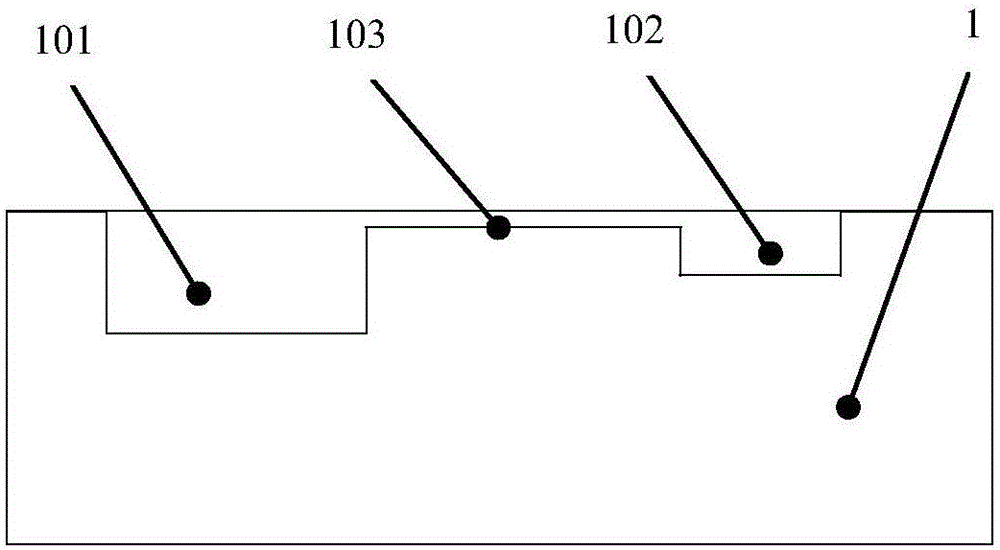
[0035] Step 2: Use a fused deposition 3D printer to manufacture electronic product structures (including basic functional structures, reserved hole structures for embedded electronic components, and reserved groove structures for connecting electronic components and connecting circuits, etc.);

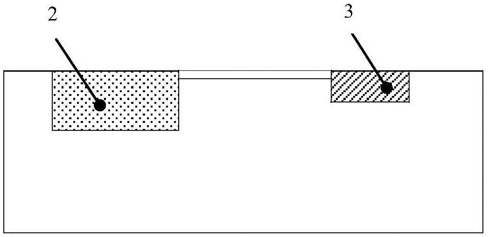
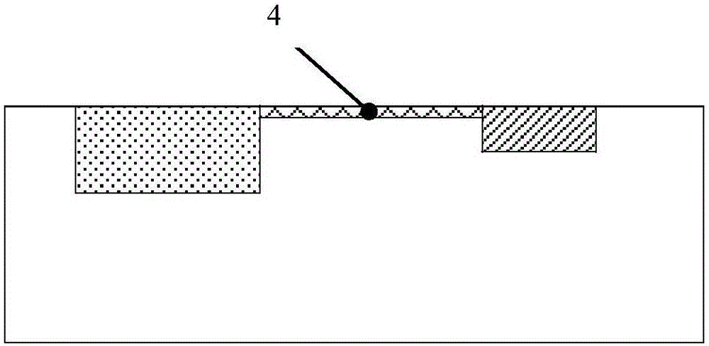
[0036] Step 3: Stop and pause the 3D printer according to the preset pause positi...


PUM


Abstract

The invention discloses a 3D printing method for an embedded electronic product. The 3D printing method for the embedded electronic product includes the following steps that firstly, a base layer and a structure layer of the electronic product are printed in a fused deposition 3D printing mode; secondly, fused deposition 3D printing is paused according to a preset pause position, and electronic elements are embedded in set positions of the structure layer; thirdly, a connecting circuit among the electronic elements is printed in an electronic injection 3D printing mode; fourthly, after the circuit is completely cured, if the electronic product is of a single-layer structure, the fifth step is directly carried out, and if the electronic product is of a multi-layer structure, the first step to the third step are repeated until printing of the last layer structure is completed; and fifthly, the top layer structure of the electronic product is printed in a fused deposition 3D printing mode, and printing of a packaging structure of the electronic product is completed. Integrated manufacturing of the high-efficiency, low-cost and high-resolution embedded electronic product is realized, and integrated manufacturing of materials, structures and elements is also realized.

Description

technical field [0001] The invention belongs to the technical field of additive manufacturing and electronic products, and in particular relates to a 3D printing method for embedded electronic products. Background technique [0002] 3D printing technology realizes the manufacture of almost arbitrary complex structures, and has been applied in aerospace, tissue engineering, biomedicine, automobiles, home appliances, new materials, new energy, robots, construction and many other fields, showing broad application prospects. With the rapid development of 3D printing technology, 3D printing has begun to be applied to the electronics industry in recent years, for flexible electronics, wearable devices, intelligent sensing, embedded electronic products, functional structural electronic The development of a new generation of electronic products such as structures provides a new manufacturing method, especially a new solution for the development and integrated manufacturing of embedd...

Claims


Application Information

Patent Timeline
IPC IPC(8): B29C67/00B22F3/115B33Y10/00
CPCB22F3/115B33Y10/00
Inventor 兰红波杨建军朱晓阳
Owner QINGDAO TECHNOLOGICAL UNIVERSITY
Why Eureka
Try Eureka