3D printing method of integrated encapsulating luminous device

A 3D printing, light-emitting device technology, applied in semiconductor devices, electrical components, ceramic molding machines, etc., can solve the problems of accelerated LED photoaging, reduced service life, hindered heat transfer, etc., to achieve good thermal conductivity, reduce Volume and weight, the effect of improving the performance of the product

Inactive Publication Date: 2019-01-25
DONGGUAN INST OF OPTO ELECTRONICS PEKING UNIV
View PDF5 Cites 3 Cited by
  • Summary
  • Abstract
  • Description
  • Claims
  • Application Information

AI Technical Summary

Problems solved by technology

However, the current ceramic metallization process can only be limited to making circuits on the front and back surfaces of ceramics (the two layers of circuits are connected by laser drilling, connected by electroplating, chemical plating, etc.), that is, only two layers can be made at most. circuit
If a multi-layer circuit is to be realized, it can only be achieved by bonding a metallized ceramic substrate. The thermal conductivity of the adhesive is much lower than that of the ceramic itself, which hinders the transfer of heat, accelerates the aging of LED light, and reduces the use life

Method used


Image

  • 3D printing method of integrated encapsulating luminous device
  • 3D printing method of integrated encapsulating luminous device

Examples


Embodiment 1

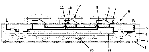
[0035] as attached figure 1 Shown, a kind of 3D printing method of integrated package light-emitting device, comprises the following steps:

[0036] S1, draw the model with 3D drawing software according to the design requirements, and convert it into a file format that can be recognized by the 3D printing equipment.

[0037] S2, use metal copper as the material to print the copper substrate 1 with the heat dissipation channel interface, the interface of the heat dissipation channel 3 is provided with threads for easy connection, print the ceramic substrate 2 with the heat dissipation channel 3 on the copper base 1, and the port of the heat dissipation channel 3 is facing The heat dissipation channel interface on the copper substrate 1, and the ceramic substrate is made of aluminum nitride. The direction of the heat dissipation channel is a composite structure of curved and straight lines, and may have a transverse heat dissipation channel 3a and a longitudinal heat dissipatio...

Embodiment 2

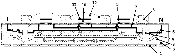
[0046] as attached figure 2 As shown, the printing steps are basically the same as in Example 1, including copper substrate 1, ceramic substrate 2, heat dissipation channel 3, electronic components 4, conductive circuit 5, bowl cup 6, power supply external pad 7, solder 9, LED chip 10 , phosphor glue 11, lens 12. The difference is that flip-chip LED chips are used. At this time, there is no need to print bonding wires, and the electrical connection is directly achieved through solder.


PUM


Abstract

The invention discloses a 3D printing method of an integrated encapsulating luminous device. The method includes the steps of designing a model, converting the model into an identifiable file format,printing a ceramic substrate with a heat dissipation passage on a copper base, printing grooves and circuit slots, printing electronic components in the grooves, printing graphene circuits in the circuit slots, printing a thin ceramic layer to cover the electronic components and the graphene circuits, and repeating the steps above according to hierarchical slicing information until printing of theheat dissipation passage, electronic components and circuits is completed; printing a wafer welding disc, an external power source connection welding disc and related surface layer circuits; printinga bowl cup, coating the inner wall of the bowl cup with a reflected layer material, printing a layer of welding material at the positions where wafers are about to be welded, and fixing the wafers through heating; printing bonding wires and fluorescent powder again and installing lenses later to complete encapsulating. The method not only greatly simplifies a traditional process, shortens the production cycle and lowers the manufacturing cost but also provides more selections for microminiaturization and complication of product size.

Description

technical field [0001] The invention belongs to the field of ceramic substrate production and LED packaging technology, and specifically relates to a 3D printing method for integrated packaging of light-emitting devices. Background technique [0002] The advent of ceramic substrate products has opened the development of the heat dissipation application industry. Due to the heat dissipation characteristics of ceramic substrates, and the advantages of high heat dissipation, low thermal resistance, long life, and withstand voltage, ceramic substrates are widely used in various fields such as LED packaging, power electronic devices, and multi-chip modules. [0003] Metallization of ceramics is to firmly adhere a layer of metal film on the surface of ceramics to realize the welding between ceramics and metals. The existing molybdenum-manganese method, gold plating method, copper plating method, tin plating method, nickel plating method, LAP method (Laser metal plating) and other...

Claims


Application Information

Patent Timeline
Patent Type & Authority Applications(China)
IPC IPC(8): B28B1/00H01L33/54H01L33/62H01L33/50B33Y10/00
CPCB28B1/001B33Y10/00H01L33/50H01L33/54H01L33/62
Inventor 杨功寿卢洪郑小平李成明王琦张国义
Owner DONGGUAN INST OF OPTO ELECTRONICS PEKING UNIV
Why Eureka
Try Eureka