3D printing method for embedded electronic product and 3D printer

A technology for 3D printers and electronic products, applied in 3D object support structures, manufacturing tools, additive manufacturing, etc., can solve the problems of support removal and inability to realize integrated manufacturing of embedded electronic products, and achieve easy removal, convenient suspension of disassembly and The effect of high installation positioning and positioning accuracy

Active Publication Date: 2017-03-15
QINGDAO TECHNOLOGICAL UNIVERSITY
View PDF10 Cites 28 Cited by
  • Summary
  • Abstract
  • Description
  • Claims
  • Application Information

AI Technical Summary

Problems solved by technology

[0004] In order to solve the above problems, the present invention proposes a 3D printing method and a 3D printer for embedded electronic products. The present invention combines Fused Deposition (FDM) and Electric Assisted Injection Deposition technology to introduce a separation between the structural material and the supporting material It provides a new type of multi-material composite 3D printing technology and equipment, realizes the integrated printing of structural materials and functional materials, effectively solves the problem of support removal in the manufacturing process of embedded electronic products, and realizes the "material-structure- "Device" integrated manufacturing, especially to realize the integrated manufacturing of electronic products with multi-layer circuit structure, which solves the problem that the existing 3D printing technology cannot realize the integrated manufacturing of embedded electronic products

Method used


Image

  • 3D printing method for embedded electronic product and 3D printer
  • 3D printing method for embedded electronic product and 3D printer
  • 3D printing method for embedded electronic product and 3D printer

Examples


Embodiment 1

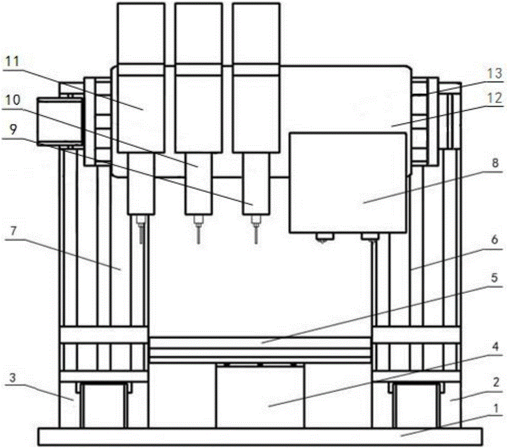
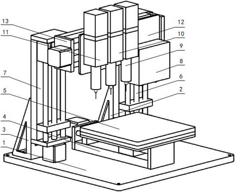
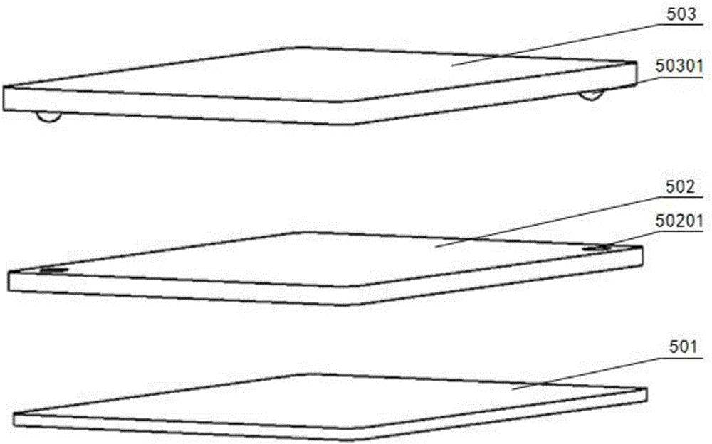
[0045] figure 1 It is a schematic diagram of the structure and principle of the 3D printer used to manufacture embedded electronic products in Embodiment 1 of the present invention, figure 2 It is a perspective view showing the structural principle of a 3D printer for manufacturing embedded electronic products according to Embodiment 1 of the present invention. Embodiment 1 The 3D printer used to manufacture embedded electronic products includes: base 1, support I2, support II3, Y-direction workbench 4, printing bed 5, Z-direction workbench I6, Z-direction workbench II7, first nozzle 8 , the second nozzle 9, the third nozzle 10, the fourth nozzle 11, the nozzle mounting plate 12, and the X-direction workbench 13. Among them, the Y-direction workbench 4 is fixed on the base 1 and is located in the center of the base 1; the printing bed 5 is composed of a support plate 501, a hot bed aluminum substrate 502 and a magnetic printing platform 503 and placed on the Y-direction work...

Embodiment 2

[0067] Embodiment 2 The schematic diagram of the structure and principle of the printer is as follows Figure 7 As shown, the electrojet printing technology is used to print conductive lines. Connecting the third spray head 10 and the printing bed 5 to the high-voltage power supply 14 can achieve higher precision of the conductive circuit.


PUM


Abstract

The invention discloses a 3D printing method for an embedded electronic product and a 3D printer. After each layer of structure material is printed, a layer of release material is arranged around a support reserved position in a jet printing manner, support printing is conducted, and when the set of structure layers are printed, supports of reserved holes and grooves are removed, an electronic component is embedded, printing of the set of electric conduction layer structure, jet printing of electric conduction circuits and jet printing of dielectric materials between the electric conduction circuits are sequentially conducted, the process is repeatedly conducted till the last set of electric conduction layer structure is printed, and the electronic product is packaged through printing structure materials. The release material is introduced between the structure material and a support material, the support material is easy to remove, on one hand, removal of the supports through an ultrasonic alkaline solution is avoided (a traditional support removing technology is not allowed to be adopted in the embedded electronic product), and on the other hand, influences on a printed electric conduction circuit from support removal are avoided. The problem about support removal in the embedded electronic product manufacturing process is effectively solved.

Description

technical field [0001] The invention belongs to the technical field of additive manufacturing and electronic products, and in particular relates to a 3D printing method and a 3D printer for embedded electronic products. Background technique [0002] Embedded electronic products (functional structural electronics) are a new type of electronic products that have emerged with the development of additive manufacturing technology in recent years. While printing the object structure, sensors, controllers, drivers, antennas, batteries and other electronic components At the same time, it is embedded into the printed structure, and some simple circuits and connecting circuits are directly printed, so as to truly realize the integrated manufacturing of functional structural electronic products, and the integrated manufacturing of materials-structure-device. Compared with traditional electronic products, embedded electronic products have some unique advantages and notable features; (1)...

Claims


Application Information

Patent Timeline
Patent Type & Authority Applications(China)
IPC IPC(8): B29C64/112B29C64/40B29C64/30B33Y10/00B33Y30/00B33Y80/00
CPCB33Y10/00B33Y30/00B33Y80/00
Inventor 兰红波刘志浩杨建军赵佳伟
Owner QINGDAO TECHNOLOGICAL UNIVERSITY
Why Eureka
Try Eureka